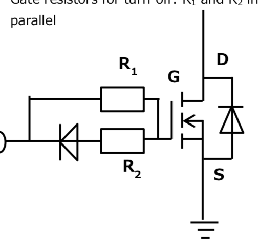
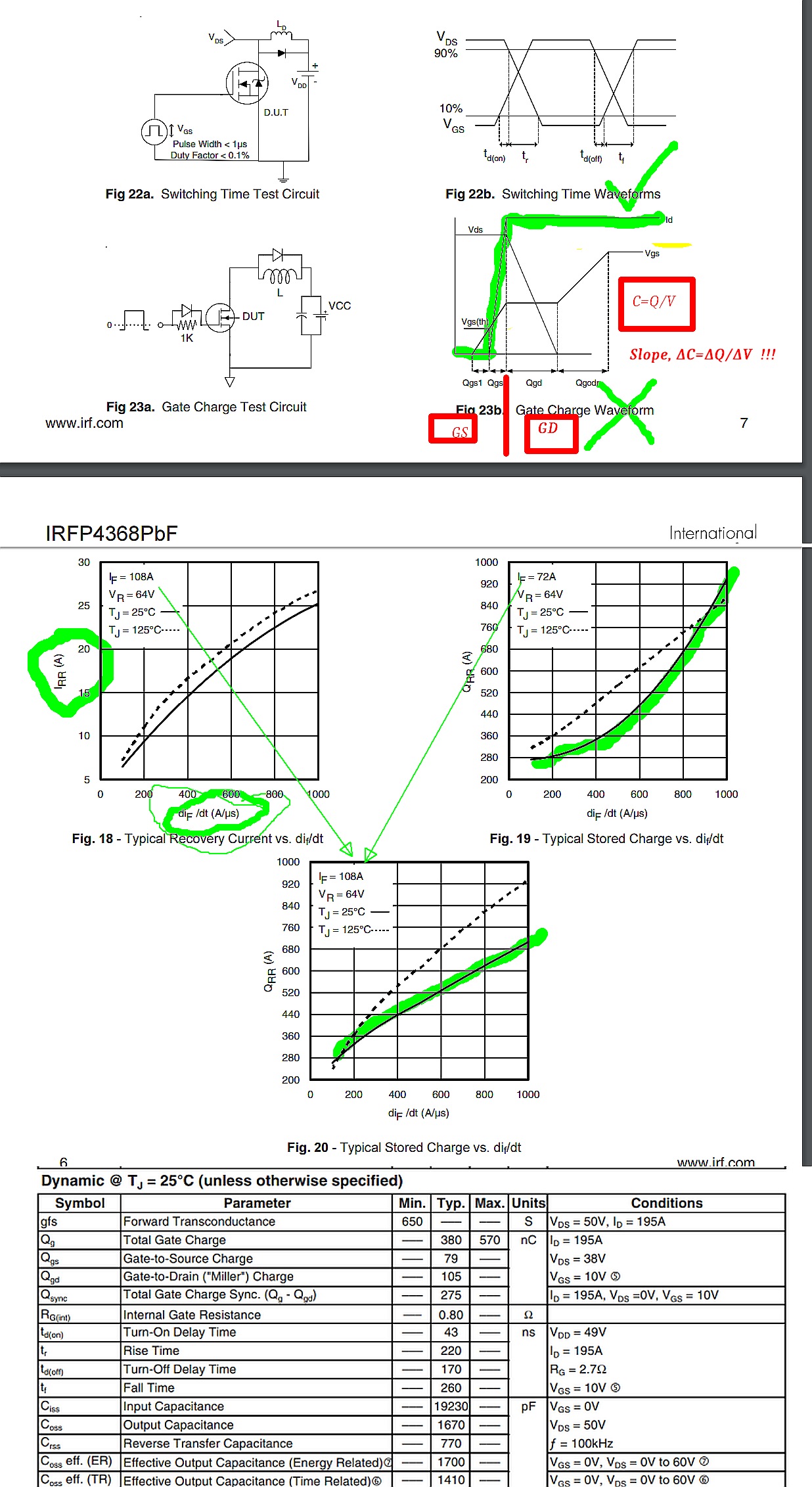
 I am using the equation Qg = ig * t in order to calculate the gate resistor which charges the MOSFETs input capacitance (Ciss). The MOSFET I am using is the IRFP4368PBF. So if I use the equation Q=CV I can find the charge, in this case being (19860pF * 15V = 297.9nC). By rearranging (Qg = ig * t) to
(ig = Qg / t) gives (297.9nC / t) . My question is that how do I find t , is it on the MOSFETs data sheet ? or else where ? because if i know t than i can calculated the current flowing into the MOSFETs gate which will than allow me to calculate the gate resistor.
-
\$\begingroup\$ You might want to look at "Total gate charge" parameter. \$\endgroup\$– Long PhamCommented Dec 25, 2018 at 15:37
-
\$\begingroup\$ I have calculated it to be 297nC \$\endgroup\$– Daniel BashyCommented Dec 25, 2018 at 16:18
-
\$\begingroup\$ I don’t really understand your question. You generally want to keep the charge time as short as possible. For that, there’s no need for a gate resistor… \$\endgroup\$– user2233709Commented Dec 25, 2018 at 16:51
-
\$\begingroup\$ If I’m missing something, I guess a schematic would help. \$\endgroup\$– user2233709Commented Dec 25, 2018 at 16:52
-
\$\begingroup\$ @user2233709 Well, as you've noted the gate behaves like a capacitor. Now here's the crazy part, wires has inductance, if you do not use any resistor anywhere then you will have a gate that is oscillating like mad every time you turn it off/on. Imagine an H-bridge where the gates are oscillating very fast, you're essentially shorting the transistors across VDD and GND with the ringing, and you are making a very noisy output. unless you use a resistor and dampen the ringing. \$\endgroup\$– Harry SvenssonCommented Dec 25, 2018 at 16:56
2 Answers
There is often confusion in reading graphs. Some show Vgs and ID vs Q in datasheets and vs t in textbooks. Meanwhile the Rd bulk resistance of the diode is unknown when rising voltage bypasses the 1K.
To me it, would make more sense to use the diode reverse both for the datasheet to match the Q and t graphs for a rising input. Also this is actually how most bridges use them. YOu want the turn ON time slower than turn OFF to create the dead-time and avoid cross conduction for some period like 1us depending on load L/RdsOn. Otherwise you up with continuous conduction in the choke and cross-conduction failure in the push-pull FETs.
Note that C rises rapidly between Vgs(th) and up to 2 to 3x this threshold where RdsOn reaches near the rated low value but not quite.
So I suggest you use the diode in Fwd Mode to turn OFF with it's bulk resistance based on power rating of the diode Rs [Ω] ~ 1/2P[Ω], (ballpark +/-50%) and the Rg selected to determine your dead time on the order of 3~5x Rs of the diode. You can add a small R in series with the diode in order to reduce the ballpark tolerances for more consistent production results.
This is not intended to give you a complete answer but more to think about. 1us depending on L can vary widely. It is typically the difference between worst case Tdt=turn {on-off} time.
It is not simply \$Q=I_g*t\$ since it is also affected by \$I_d=C_{gd}*dV_{gd}*dt\$
-
\$\begingroup\$ I have edited the digram so it charges through R1 and discharges through both R1 and R2, my teacher said use the equation (Qg =iG*t ) to calculate the resistor values and just said put 1us for t. i don't understand why 1us and is that just an assumption \$\endgroup\$ Commented Dec 25, 2018 at 19:00
-
\$\begingroup\$ which part do you not understand on my answer? \$\endgroup\$– D.A.S.Commented Dec 25, 2018 at 21:35
I don't want to make this a one-link answer, so I'll write a quick summary, but you should really read this appnote.
If I use the equation Q=CV I can find the charge
Not really. MOSFET capacitance varies with Vgs and Vds. Also, a large part of the gate charge is due to miller effect through Cgd:
First the FET is OFF, and Vds is usually equal to the supply voltage Vcc. Then, gate voltage rises as current charges Cgs. Once threshold voltage is reached, the FET begins to conduct, and Vds goes down. This causes the voltage across Cgd to vary, and a capacitor with varying voltage across it implies a current. Thus the driver has to inject all the charge required to bring the voltage across Cgd to its final value. Once the FET is fully ON, Vds is quite small, and then gate current is once again used to ramp up Vgs and reduce RdsON.
During switching, Cgd varies a lot depending on Vds, so you cannot use Q=CV which implies a constant capacitor. You must use datasheet values instead, or simulation with accurate models.
Total gate charge will depend on final Vgs, but also on initial Vds (=supply voltage). Your calculation ignores Cgd, so you are under estimating Qg.
Now your original question about the gate resistor value. It's a bit complicated. Higher resistor value will slow down turn-on but calculating how much time it will take to charge the gate up to Qg is always a big approximation as the MOSFET gate is not a constant value capacitor, and the MOSFET driver usually outputs a voltage, so using a fixed value resistor will result in high current during the beginning of turn-on, but as gate voltage increases then current will get lower... like in a RC circuit.
The purpose of the gate resistor is to prevent MOSFET oscillation, slow down switching if you want to avoid EMI problems, stuff like that. If you use a low frequency then slowing down the switching is an excellent way to reduce EMI. Some circuits use different resistors for turn-on and turn-off, with diodes or a dual-output driver ; this is a way to adjust switching times to avoid cross-conduction when using two FETs in synchronous mode.
So the value of the resistor depends on what its intended use is... which you don't tell.
-
1\$\begingroup\$ Comments are not for extended discussion; this conversation has been moved to chat. \$\endgroup\$ Commented Dec 27, 2018 at 17:31


