5
\$\begingroup\$

part identification question here. It comes from an Xfinity XR11 Remote. It’s used to detect acceleration when picking up the remote.
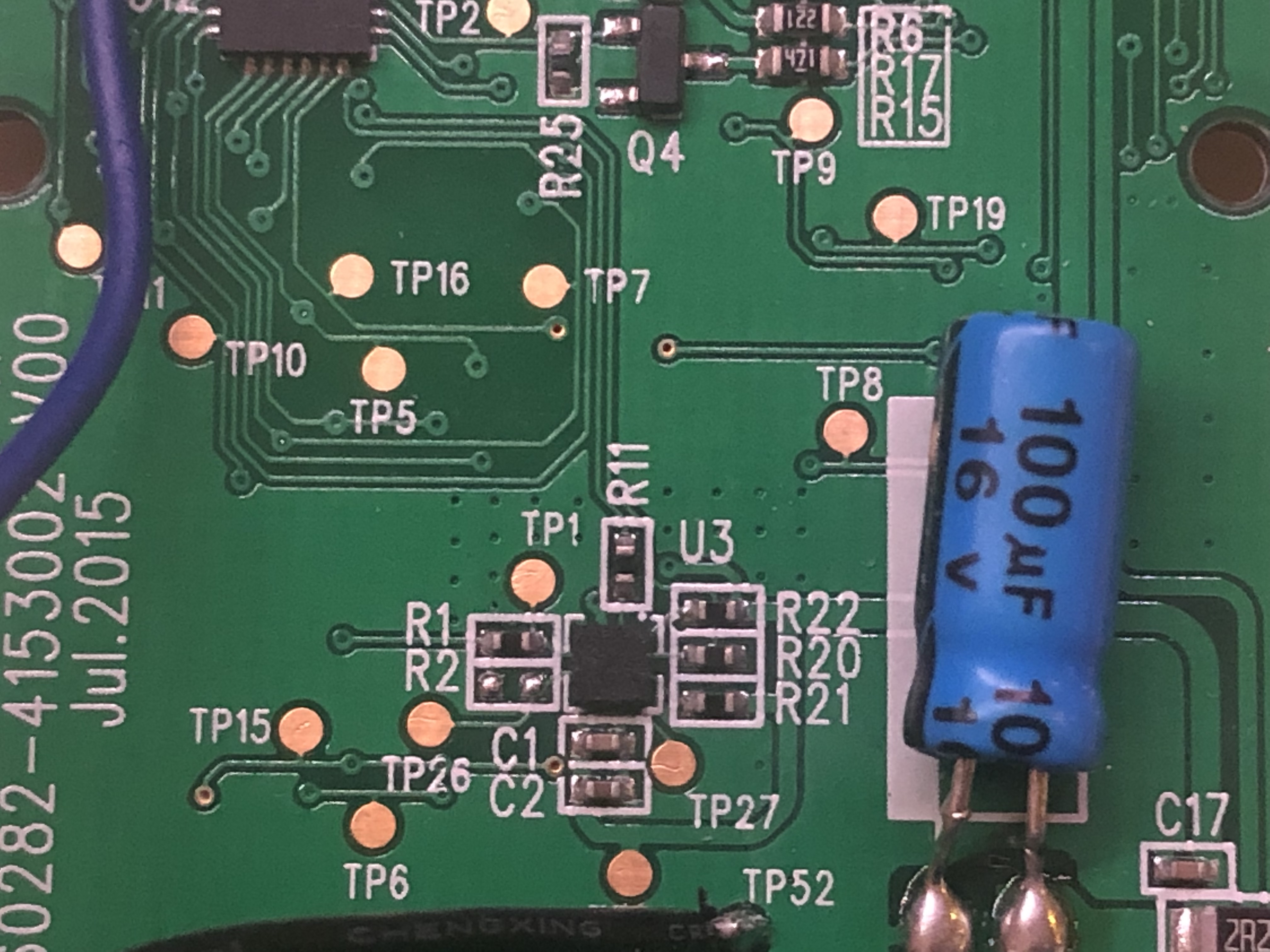
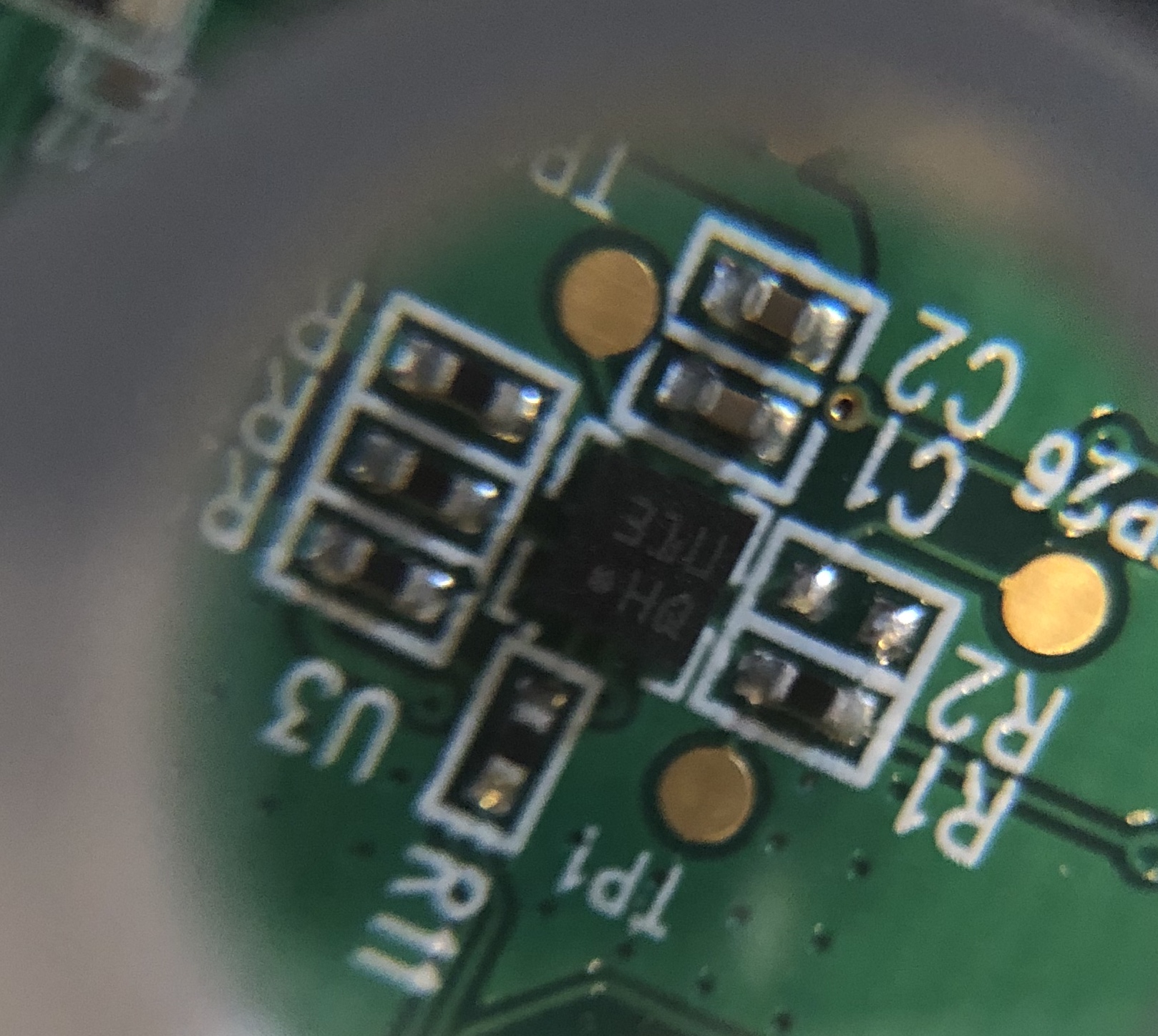
Position on board Package Closeup

The footprint and part/trace placement heavily matches what I’d expect for an STM accelerometer but the register map just doesn’t fit. Specifically one of these.

The package reads 31UHQ and is a 2mmx2mm LGA package. It seems that the 4x3 pin layout has a standard pin configuration of two interrupt outputs and I2C/SPI pin locations.

It has registers starting at 0x00 and some of the reads and writes I see from a logic analyzer are to addresses that the datasheet claims are “reserved”. For example, bits 0, 1, and 2 on register 0x17 enable the X, Y, and Z axis. I can provide a full register dump if needed.

If it helps, here are the ins and outs. All resistors are 0ohm bridges.

  • R11 = SCL
  • R20 = SDA
  • TP50 = VCC (2v5)
  • TP1 = Interrupt (not sure if INT0 or INT1)
  • TP26 = Unknown
  • TP27 = Unknown

Start-up sequence: (Op, Reg, Data)

  1. W 17 07
  2. W 19 02
  3. W 25 04
  4. W 26 06
  5. W 36 07
  6. W 20 08
\$\endgroup\$
4
  • \$\begingroup\$ Interestingly they’re only using the interrupt line and never read from the device. \$\endgroup\$ Commented Dec 28, 2018 at 2:46
  • \$\begingroup\$ At least give the dimensions, pin count and pinout!! And what is your actual goal here?? \$\endgroup\$ Commented Dec 28, 2018 at 3:46
  • 1
    \$\begingroup\$ Unknown, assuming 12 pins, fun!!?? \$\endgroup\$ Commented Dec 28, 2018 at 7:07
  • \$\begingroup\$ To be a little more serious, because I can’t desolder the chip I can’t be sure, but if you follow the link I provided and check out the example circuit, the placement of the external I/O matches very closely to what the pinout if a LIS331DLH would be. For the goal, I just felt like writing some device drivers in Rust and this is the last component I need to figure out before tearing off the SoC: gist.github.com/RandomInsano/49148e290b5b3d8650b0d600c3e2dd2b \$\endgroup\$ Commented Dec 28, 2018 at 7:23

1 Answer 1

4
\$\begingroup\$

Okay, after much digging it is a BMA222E. I got hung up on a specific pin layout of 12 pin LGA packages, but I focused instead on the size of the package (thanks chris-stratton for making that important).

My test for the chip after confirming all of the register addresses mapped to existing user addresses was to write to one of the eight non-volatile EEPROM registers, shut the chip down, then re-read the registers. Sure enough, the data is still there. Second confirmation was that the CHIP_ID value was correct.

For others trying to do this sort of identification in the future, only the 'H' on the laser etching has anything to do with the part and in newer iterations of the same chip there is nothing to tell them apart.

Also, many accelerometers share the same pinout and footprint which means the register layout and chip identifiers are the only reasonable ways to identify the part you have. Legwork on Mouser and Digikey are a must for these parts and using the package type and pin layout lets you filter your search.

The upshot of the shared landing design is that is that vendor lock-in here is minimal in designs! It also explains the number of jumpers around the package in my exhibit above: Just bridge the right pins for the job.

\$\endgroup\$

Your Answer

By clicking “Post Your Answer”, you agree to our terms of service and acknowledge you have read our privacy policy.

Not the answer you're looking for? Browse other questions tagged or ask your own question.