1
\$\begingroup\$

I have a project that's using an IC that only comes in SMD packages. With my limited soldering experience, I think I could potentially solder a TSSOP, but I think QFN is well beyond my capabilities.

I decide to try to make a PCB that adapts the TSSOP to a DIP profile compatible with common breadboards.

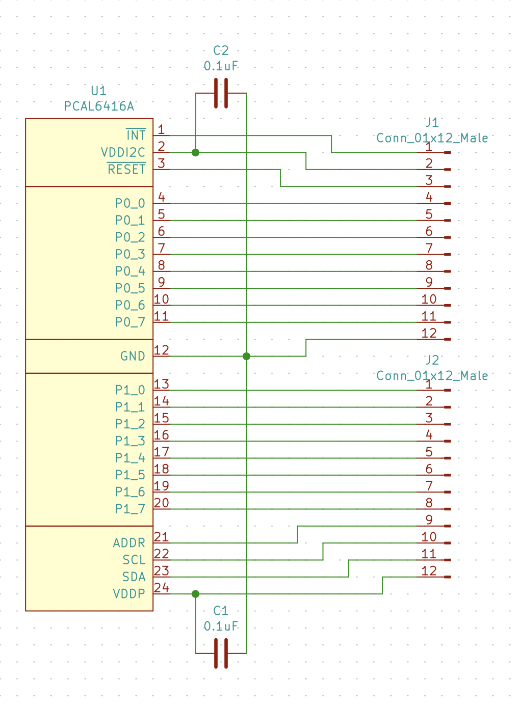
This particular IC (NXP PCAL6416A) has two supply pins, one for the I2C bus and one for the GPIO ports (this is an IO expander).

Would this capacitor placement and configuration potentially work for decoupling my two supply pins? Would it be a problem if both pins are on the same supply line vs. different ones?

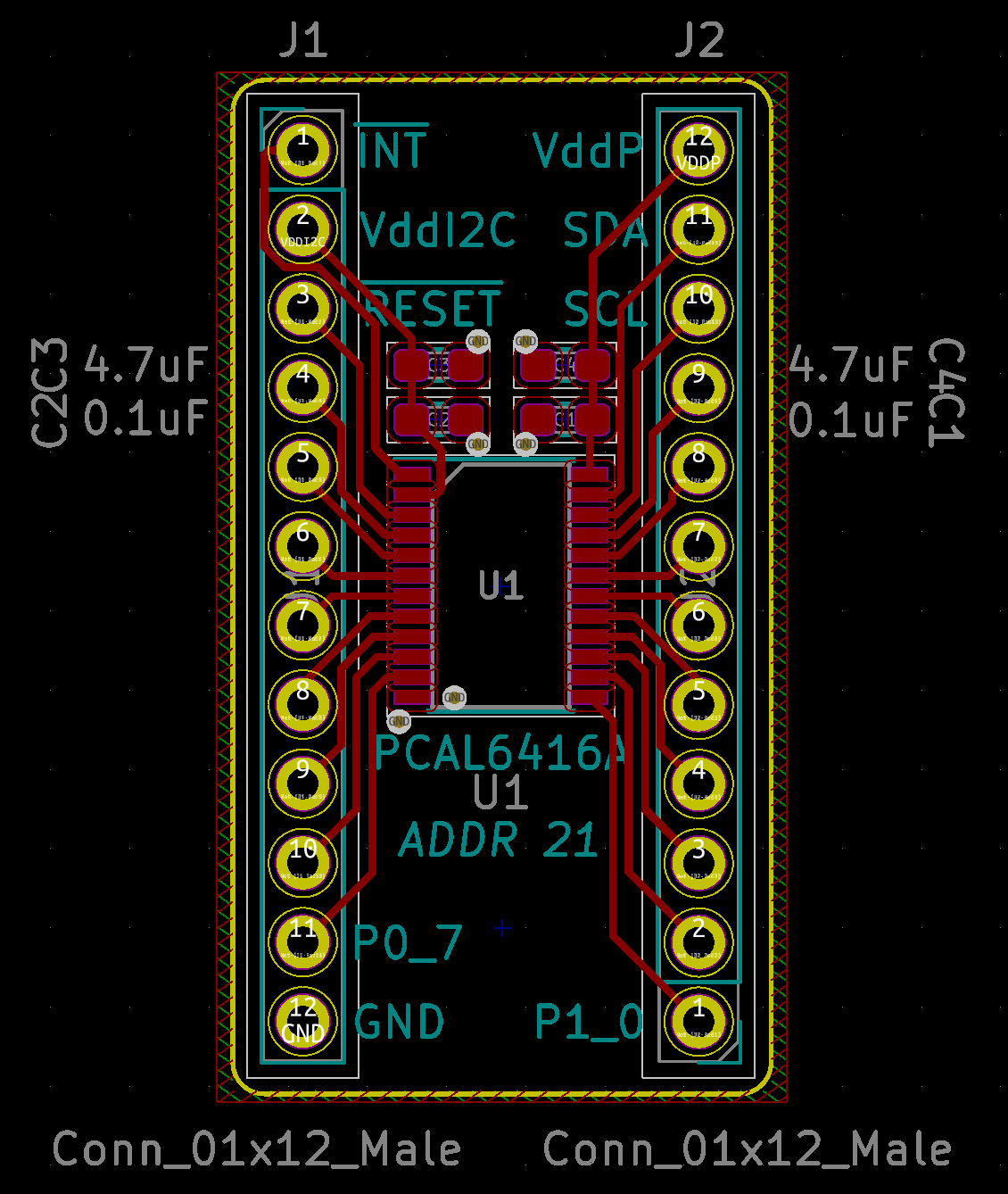
This is the PCB layout:

PCB layout

This is the schematic:

schematic

Thanks very much!

Edit:

In case other hobbyists come across this question and would be helped by a visual representation of the answer, here's the latest implementation I have based on my understanding of the solution:

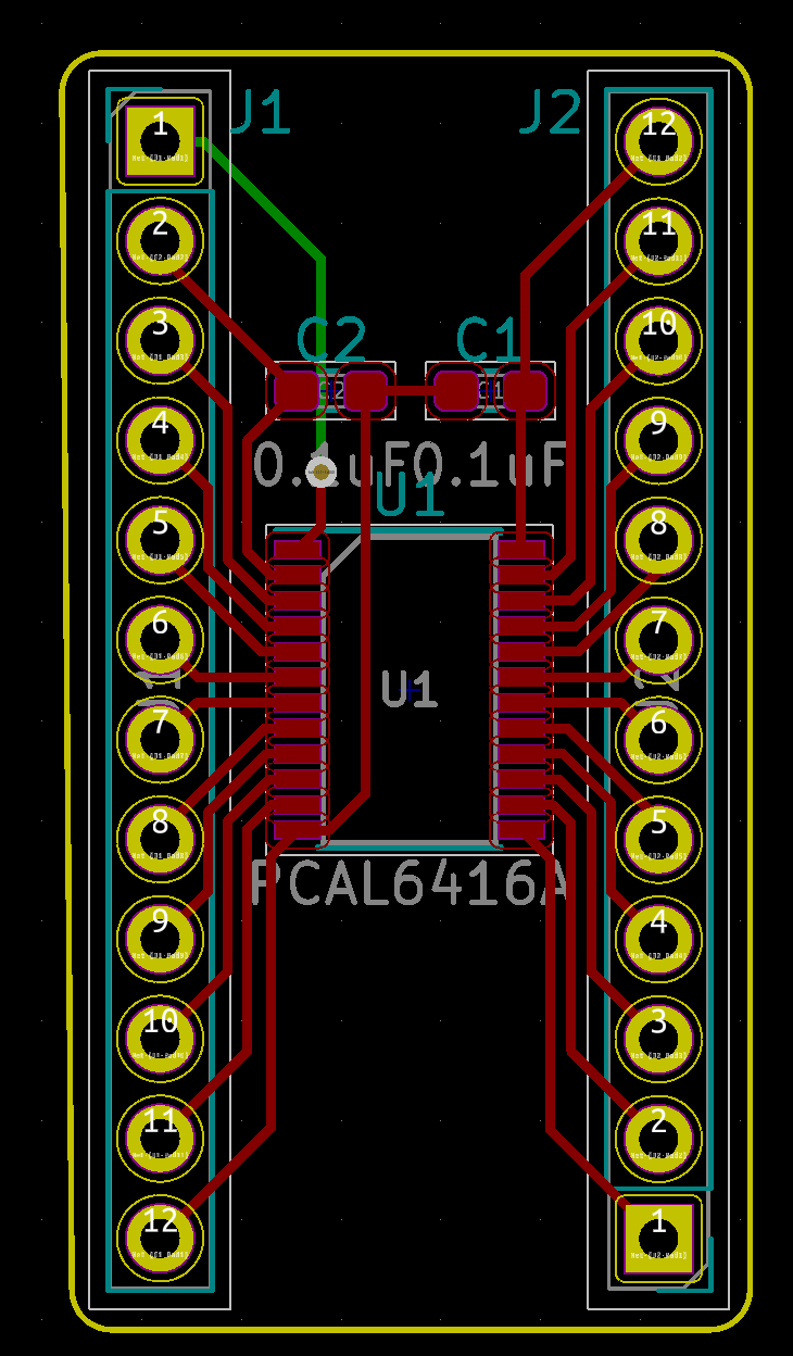
enter image description here

\$\endgroup\$
9
  • 1
    \$\begingroup\$ Normally what you have would be minimal. Adding 4.7uF MMC capacitors somewhat close to the IC helps to filter lower frequency noise. They must have low ESR specs to be useful. \$\endgroup\$
    – user105652
    Commented Jan 5, 2019 at 7:23
  • 4
    \$\begingroup\$ It is a very sub-optimal layout. Since you have a 2-layer board, dedicate one layer to mostly ground, place C2 below the IC, and ground C1 with via. Same supply or different - it doesn't matter. But currently both bypass caps share a very long common trace, and a sizable cross-talk between two rails is guaranteed. \$\endgroup\$ Commented Jan 5, 2019 at 7:48
  • 1
    \$\begingroup\$ @Ale..chenski I'd argue that in this board, having a ground plane on the top layer and the caps on that same layer would be advantageous to avoid via inductance, since the IC pinout allows for caps to be placed very near to the pins (shift U1 slightly to the right, so that C2 fits left of it). Bottom ground plane is of course the way to go, no matter what you do. \$\endgroup\$ Commented Jan 5, 2019 at 9:59
  • 2
    \$\begingroup\$ @MarcusMüller why don't you post as an Answer ? \$\endgroup\$
    – Damien
    Commented Jan 5, 2019 at 11:13
  • 3
    \$\begingroup\$ The unaligned outline bothers me a lot! Please use the grid when drawing the outline! \$\endgroup\$
    – pipe
    Commented Jan 5, 2019 at 12:01

2 Answers 2

7
\$\begingroup\$

Pretty much anywhere, ground planes are desirable. Your km-long GND trace is no good! There will be plenty of inductance here, and the fact that you connect the two capacitors more in series between the two supply pins than in parallel to ground means that there will be coupling of noise from one to the other supply pin!

This looks like Kicad, so use the Zone tool to define a plane in the GND net, on both the top and bottom layer of the board, covering the full area of the board.

Your goal is to get the capacitors as close as possible to the supply pins. So, move them directly adjacent to the IC package.

Instead of routing INT on the bottom layer, simply route the VDDI2C right of the pad (i.e. below the package, but on the top layer) and simply route the INT between the holes of the pin header. That way, you get a continous ground plane on the bottom.

Throw in a dozen or two of ground-plane-stitching vias between the bottom and top ground plane.

As @Sparky256 pointed out, for chips that switch fast or high currents, you basically can't have too much capacitance stabilizing the power supply. So, add some additional capacitance – Sparky recommends 4.7 µF multilayer ceramic, but if that's too expensive or hard to get, I've had good experience with 1 µF ceramic + 10 µF (or more) low-ESR electrolytic / tantalum.

\$\endgroup\$
11
  • 2
    \$\begingroup\$ Considering that this is just an I/O expander with maximum currents of 20mA and being controlled via rather slow I2C, 4.7uF or 10uF is a bit overkill. \$\endgroup\$ Commented Jan 5, 2019 at 14:44
  • 3
    \$\begingroup\$ @D.Patrick unpopulated parts are rather common for many reasons. As long as placing them does not lead to problematic compromises, e.g., adding excessive trace parasitics due to increased part separation, then there would be no issues. \$\endgroup\$ Commented Jan 5, 2019 at 15:58
  • 1
    \$\begingroup\$ … and that wouldn't happen here, since this is a low-frequency circuit, not something in the upper MHzes. \$\endgroup\$ Commented Jan 5, 2019 at 16:16
  • 1
    \$\begingroup\$ yep, and aside from "if in doubt, add one", I honestly wouldn't know well! I'd be very interested in the answer to that question! \$\endgroup\$ Commented Jan 5, 2019 at 18:29
  • 1
    \$\begingroup\$ looks fine to me! \$\endgroup\$ Commented Jan 5, 2019 at 21:13
1
\$\begingroup\$

Two important factors are ;

  • external power sequencing synchronization
  • on board ground plane for reducing inductance noise

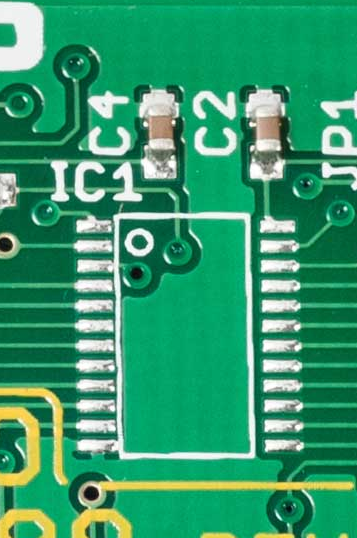
This would look better.

enter image description here

\$\endgroup\$

Your Answer

By clicking “Post Your Answer”, you agree to our terms of service and acknowledge you have read our privacy policy.

Not the answer you're looking for? Browse other questions tagged or ask your own question.