0
\$\begingroup\$

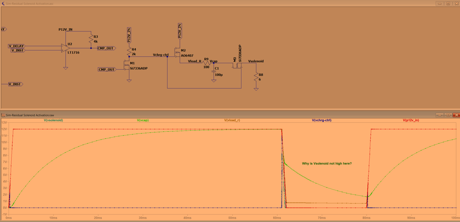
I am trying to do a charging and a discharging Circuit. R8 is the load that Capacitor C1 needs to discharge into when P12V_IN is low.

My question is Why is Vsolenoid low in the interval shown on the waveform when P12V_IN is low? I am expecting that P-FET M2 is OFF during this time so the voltage/charge of C1 should discharge into R8 since NMOS M3 is ON.

I am sure I am screwing up somewhere silly.

enter image description here

\$\endgroup\$
1
  • 2
    \$\begingroup\$ Please don't take a photo of the screen. You can export decent graphics from LTspice. \$\endgroup\$ Commented Jan 11, 2019 at 2:00

2 Answers 2

1
\$\begingroup\$

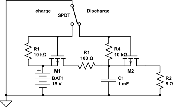
You must use two Pch FETS to make high side switches to charge and discharge.

schematic

simulate this circuit – Schematic created using CircuitLab

Otherwise V discharge needs to be 2.5Vgs(th) greater than V+. for an Nch FET. This is often done in half bridges using low side PWM and a boost negative clamp cap ac coupled to a diode to V+ to raise the gate driver voltage.

However this still may not do what you want.

How much energy do you need to move the solenoid depends on force and distance as well as current and time duration.

If your 6 Ohm load is 1 Henry, You might need 1 Farad to power it. Then if there is an opposing spring force , it will retract depending on the reactive:resistive time constant.

\$\endgroup\$
0
\$\begingroup\$

I believe that if you place M3 underneath R8 (M3-source connected to ground, and M3-drain connected to R8) your circuit will work.

As sunnyskyguy mentions, it has to do with high/low side switching. And yes you might need a great deal more capacitance.

\$\endgroup\$

Your Answer

By clicking “Post Your Answer”, you agree to our terms of service and acknowledge you have read our privacy policy.

Not the answer you're looking for? Browse other questions tagged or ask your own question.