I will not have time to explain everything. But feel free to tell ask another question with more background design info.
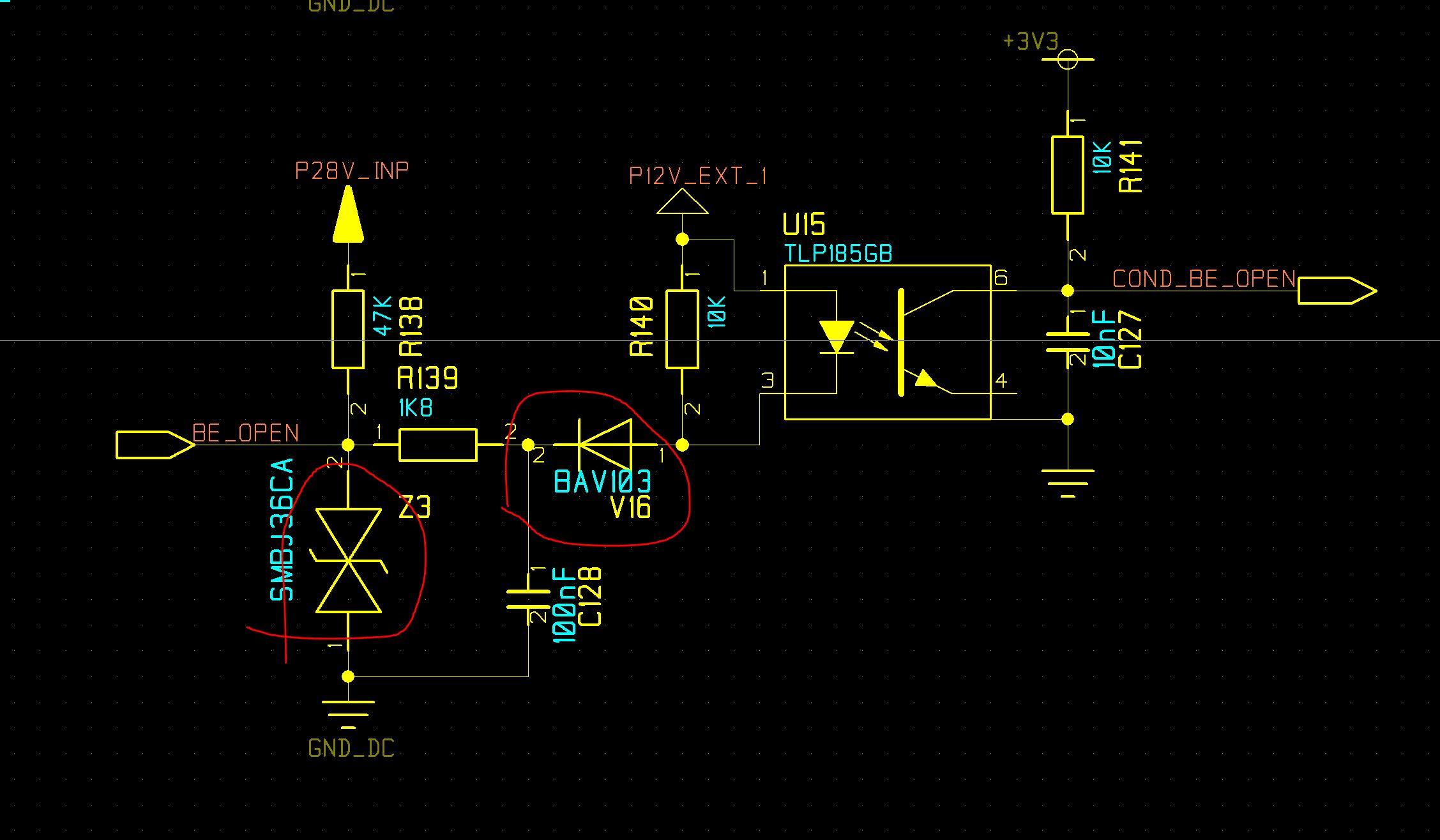
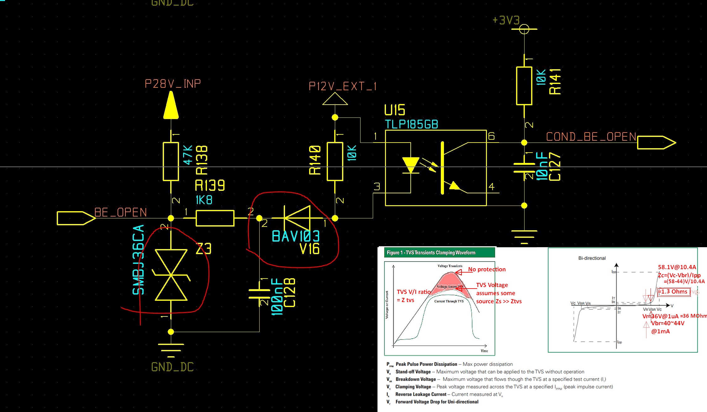
But the CA type TVS is a special dual zener back-back diode.
 The TVS acts a brute force 600W absorbing bipolar zener. But this can lead to crosstalk with leakage crosstalk current. A complete analysis is not possible without geometric layout. Basically, a good design but might still cause glitches.
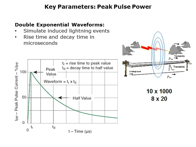
Ref  Peak pulse power ratings are measured by using laboratory-generated pulses that are designed to simulate pulses on cables caused by nearby lightning strikes. These waveforms are called double exponential waveforms. A standard waveform used in telephone circuits is a 10 x 1000 μs waveform meaning 10 μs rise time and 1000 μs tail decay time to 50% V. AC powered industry uses shorter transients (with lower impedance) which are often tested with 8 x 20 us surge impulses. Often power transformers can pass thru this voltage if the level exceeds the supply protection or is capacitively coupled or the impulse might be induced via the building lightning rod current travelling down (hopefully) not too near the elevator shaft.
A long elevator sensor-cable looks like a great antenna, so low impedance and filters are needed to attenuate RF and surge impulse noise but not too low that it conducts 100A!
The wave is defined by the Vpk, Tr, Td or sometimes Isc. The test requirements are often dictated by Industry safety standards 1st then regional standards, then national std. then international std. Sometimes it is defined by Voc and other times by Isc, short-cct.
Both modes have been supported by TVS's due to very high dynamic range (<<1uA to >10A), fast response time and low resistance. Note that these waveforms are not power waveforms. They are either voltage or current waveforms. To measure peak pulse power, the voltage and the current must both be measured and the peaks multiplied together to get the peak pulse power.
N.B.
In order to attenuate the input applied pulse, the input transient must have an impedance much higher than the TVS. However if this results in a high slew rate current, circuit layout and filters mus prevent crosstalk to nearby high impedance isolated outputs that are unbalanced.
The TVS incremental resistance, Zs at 58V = 1.3 Ω min. ( see graph text added)
This TVS is rated for 600W peak pulse power capability at 10/1000μs wave meaning 58V @ 10.4A.
IF a 10A pulse was induced in the TVS, to an optically isolated external DC path, there is still a risk of crosstalk in the supplies, ground planes and proximity to the 10k (R41) pullup , so a shunt capacitance, C127 reduces slew rate to 10nF*10kΩ = 100us is this can result in logic level glitches unless your signal/ground paths are carefully designed to not cause reactive crosstalk with the isolated 3.3V signal ground. This means the 36V and 24V are isolated except for some unknown leakage capacitance and inductance and the crosstalk must be less than exceed Vcc/2R = 3.3/20k = 165uA here or >100 db down from a 10A input pulse !!
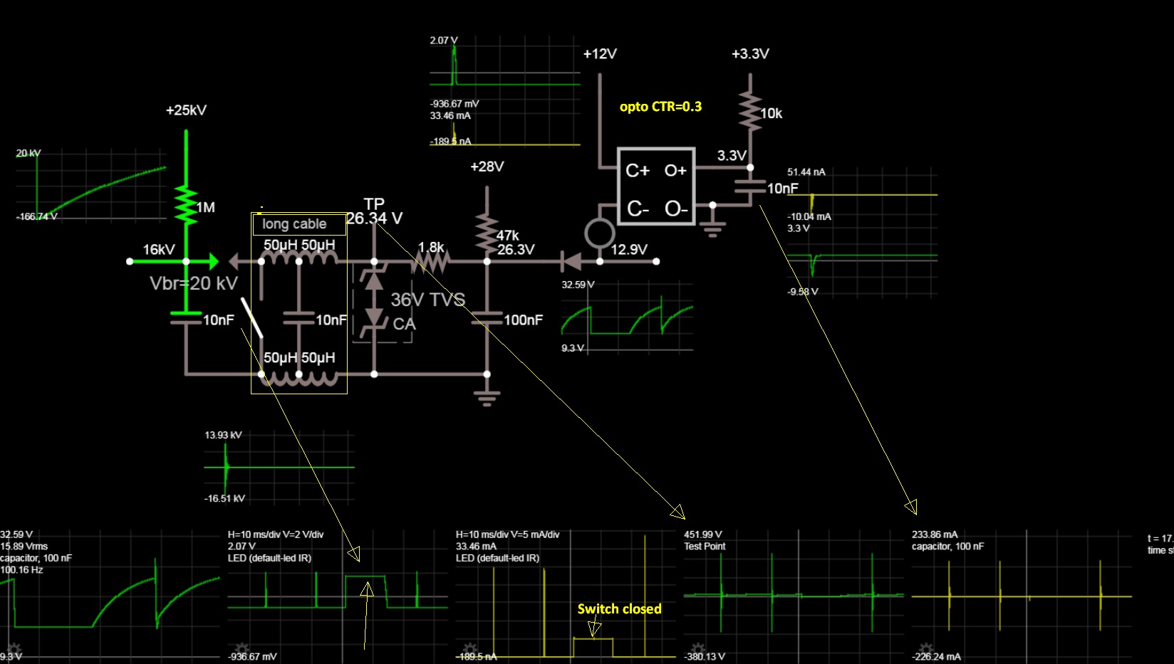
This is one attempt to simulate repeated injected impulse voltage dumped from 10nF cap thru a spark gap. The Opto was defined as a Current controlled current source with gain =CTR=0.3

This best attenuation is the 100nF cap which ought to be increased to >=1uF ceramic with a film cap to shunt piezo effects.
HERE is my old explanation of how CMOS ESD protection works. A large cap after the 1st 10K would help in this case doing similar with HV WW resistors and film caps in 2 stages with Sch. diodes so the series R to diode R ratio is about 10k:100R for a chip ESD diode and 10k:5R for a discrete 250mW Schottky diode. This "can" provide robust protection with low current 2 stage clamps, and shnt cap with ferrite beads, if done right.

