I have asked about this before but I have to admit that I didn't read enough before asking and therefore was'nt able to ask the question properly. I hope I am now.
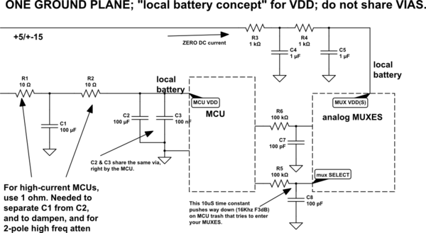
I'm designing a 4 layer board with 46 analog inputs (rotary and slide potentiometers) and 45 digital inputs (momentary push buttons). The board is controlled by a teensy 3.6. I'm using 8-channel multiplexers (M74HC4851, datasheet) since the teensy doesn't have enough inputs. The multiplexers are decoupled by a 0.1uF cap each close to their vcc pin.
I'm wondering how I should shape the ground layer. I know that the most common advise in this forum is to not shape it at all and arrange the components in a smart way instead but since my layout ist mostly determined by the hardware user interface this is not really an option in my case.
Option a)
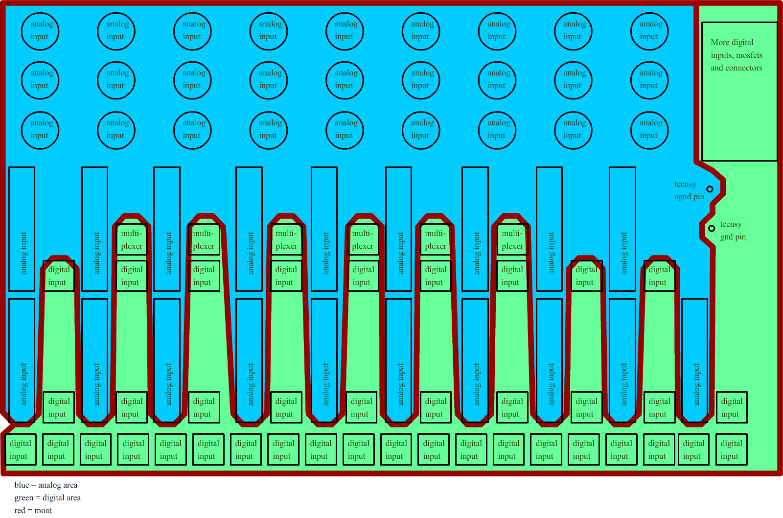 My first idea was to separate the analog area from the digital area completely by a weirdly shaped moat and connect the analog area to teensy's agnd pin, but I learned that it's not a good idea to let signal lines cross that moat and every single analog component is connected to the multiplexers which are probably the noisiest components on my pcb.
Option b)
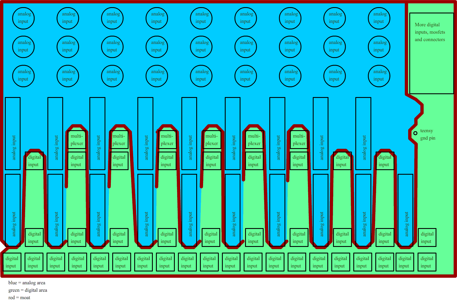 My second idea was to use several moats to force the digital return currents to not cross the analog area but then I wondered if this wouldn't create several ground loops on my board. In this case (and the following cases) I wouldn't use the agnd pin of the teensy at all.
Option c)
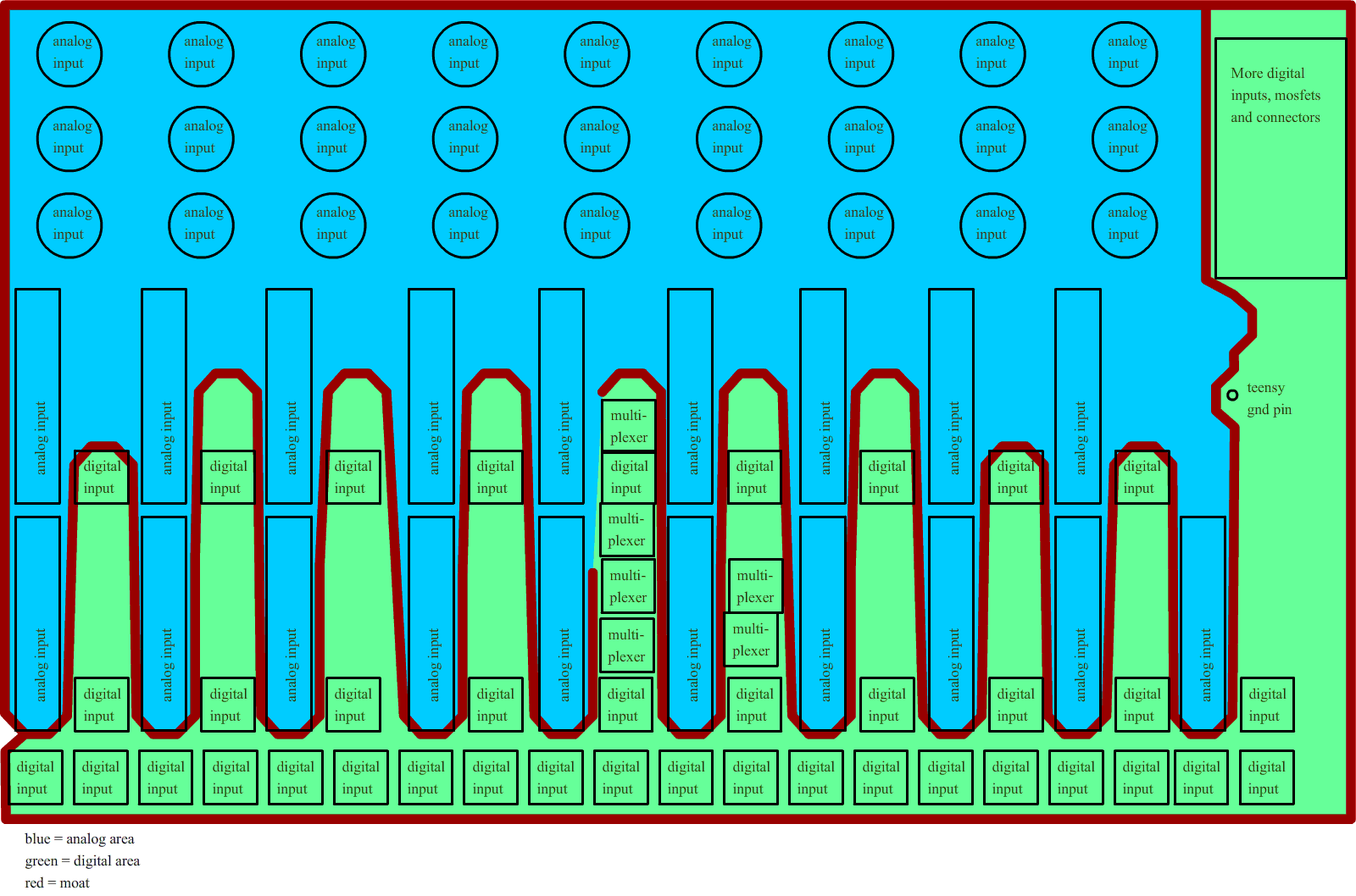 I could leave only one opening in the moat, put the multiplexers close to it and guide all signal lines through this opening (on their own layers of course) but this would make routing rather complicated and lead to rather long signal lines (the board is 35 by 23 centimeters or 13.3 by 9 inches)
Option d)
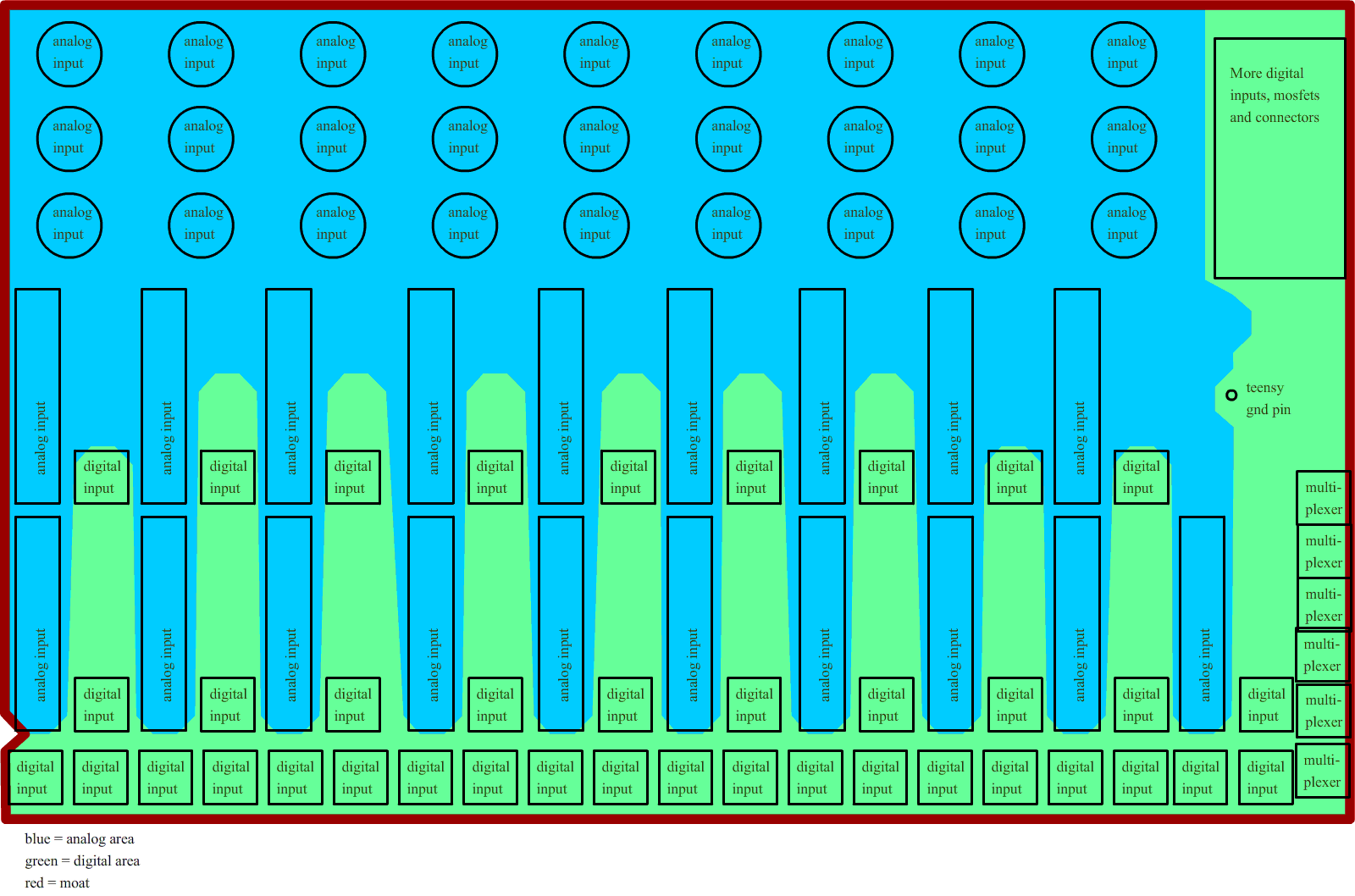 My last idea was to use one solid plane and move the multiplexers to a remote area on the board. This would have similar downsides as option c) and wouldn't control the return currents of the push buttons at all.
What's my best option? What would you do? (If moving the input components was not an option)
I'm sorry for my probably very noobish approach and thankful for your answers in advance!

