0
\$\begingroup\$

The TXS 0108E is a level shifter circuit, performing, in my project, a shift level voltage from 3.3V to 5V . Because of a design error in the wiring diagram, I left some pins with the same name on the connectors and their respective sides of the TXS 0108E IC. Not all pins, only 4. The result was that these 4 I/O pins now are connected in the pcb.

These interconnected pins are not required and are not used in the circuit, so that on both connectors, these pins will be left unconnected.

However, I can not predict if there is a problem in leaving the pins on the A and B side of the TXS0108E connected, and if this can interfere with other signals making noise or reducing the life time of the IC.

Below is a diagram of the internal circuit of the TXS0108E IC enter image description here
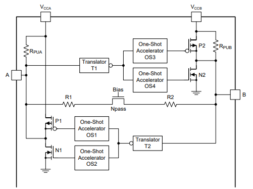
Does some one has any idea of what can happens ?

[edited]

I noted that a current will flow from Vcca to Vccb once Vcca > Vccb. But, which kind of damage it can cause ?

\$\endgroup\$
2
  • 1
    \$\begingroup\$ This is not a popular IC to use. Direction depends which side has a change of state, so this IC assumes that is the source of data at that moment. It needs to have 'dead-time' else you can have a collision with unknown results. \$\endgroup\$
    – user105652
    Commented Mar 30, 2019 at 22:40
  • \$\begingroup\$ @Sparky256 , you said that "Direction depends which side has a change of state" in general or only when I short pins of port A and B ? \$\endgroup\$
    – Daniel
    Commented Apr 2, 2019 at 16:37

1 Answer 1

1
\$\begingroup\$

Per the datasheet:

VIH High-level input voltage, A-Port I/Os:

VCCA (V) = 1.2 to 1.95, VCCB (V) = 1.65 to 5.5 :Max Vin = VCCI

VCCA (V) = 1.95 to 3.6, VCCB (V) = 1.65 to 5.5 :Max Vin = VCCI

VCCI is the VCC associated with the data input port.

:

The TXS0108E device is a directionless voltage-level translator specifically designed for translating logic voltage levels.

The A-port accepts I/O voltages ranging from 1.2 V to 3.6 V. The B-port accepts I/O voltages from 1.65 V to 5.5 V

:

Each A-port I/O has a pull-up resistor (RPUA) to VCCA and each B-port I/O has a pull-up resistor (RPUB) to VCCB. RPUA and RPUB have a value of 40 kΩ when the output is driving low. RPUA and RPUB have a value of 4 kΩ when the output is driving high. RPUA and RPUB are disabled when OE = Low.

So I would suggest just grounding the pins if they are not being used.

\$\endgroup\$
6
  • \$\begingroup\$ your suggestion is to grounding the pins of port A and B that are connected with each other ? Or to ground whatever pins that will not be used ? \$\endgroup\$
    – Daniel
    Commented Apr 2, 2019 at 16:17
  • 1
    \$\begingroup\$ Yes, ground the connected pins that are unused. Yes, ground unused inputs so they do not have a chance to float. \$\endgroup\$
    – CrossRoads
    Commented Apr 2, 2019 at 17:52
  • \$\begingroup\$ I understood. I will remake the design and I'm planning use it to different situations. One of them use only some pins the other use all of them. So, in the first situation I will have floating pins. Would be it a problem? I didn't understood why. \$\endgroup\$
    – Daniel
    Commented Apr 2, 2019 at 18:00
  • 1
    \$\begingroup\$ Grounded inputs enable the higher resistance pullup resistor, thus lower power draw. Also, grounded inputs will lead to a low output. Inputs held to a level will not float and oscillate between high and low or in between, causing unintended internal oscillations and higher current draw and/or inintended RF emissions. Lots of good reasons to hold unused inputs to a known level. \$\endgroup\$
    – CrossRoads
    Commented Apr 2, 2019 at 18:39
  • 1
    \$\begingroup\$ Just connect them to Gnd, no resistor needed. \$\endgroup\$
    – CrossRoads
    Commented Apr 2, 2019 at 18:39

Your Answer

By clicking “Post Your Answer”, you agree to our terms of service and acknowledge you have read our privacy policy.

Not the answer you're looking for? Browse other questions tagged or ask your own question.