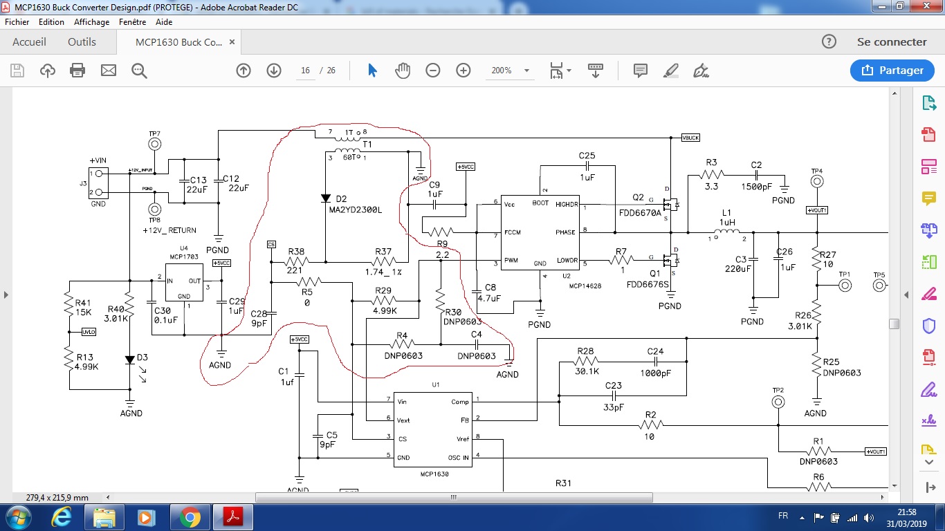
There is a Typical Application Schematic in the datasheet of the MCP14628 which uses a MCP1630 as in your schematic.
The current is sensed through the transformer T1 and goes through the diode D2 and mainly through R37, which converts the current to a voltage. At first glance, R38 and C28 form a RC filter, hence the squared CS (current sense) node. At first glance, because C5 is in parallel with C28 due to R5 being 0 ohm.
Note this RC filter hardly does anything, as its cutoff frequency lies at 40 Mhz (using both C5 and C28).
The Vext of MCP1630
is an external driver output pin, used to determine the power system duty cycle.
For high-power or highside drives, this output should be connected to the logic-level
input of the MOSFET driver.
which is the MCP14628.
- I can't figure what the application of R29 is. It is certainly not to construct a ramp signal with C5 (and C28). It's more likely the idea of R4 and C5 (and C28) is to form an averaging filter which increases the biases of the CS pin of MCP1630 at higher PWM. But again, with a cutoff frequency at 1.8 MHz (using both C5 and C28) it will fail that purpose.
I doubt the circuit is driven at a frequency higher than 1 MHz, but the screen dump doesn't reveal the connection of the OSC IN pin.
EDIT after reading MCP1630 DUAL BUCK
REFERENCE DESIGN
I think Figure 1-1 and the board layout confirm point 1 above.
In the schematic they inserted the R38 C28 filter and moved the CS node. In the board layout D2, R37 and R38 C28 are very close to each other and CS runs with a trace to R5.
NB There are quite some differences between schematic and BOM. DNP0603 suddenly appear being populated/valued, R5 appears to be 221 ohm, C5 has been doubled, etc.
I still couldn't find information regarding switching frequency, but if it is indeed > 1 MHz, I think you're right R29, C5, R5, C28, R4, C4 and R30 construct a ramp generator signal.
Also, at that frequency R38 C28 (and R5 and everything behind it like C5 and C4) will act as filter.

