0
\$\begingroup\$

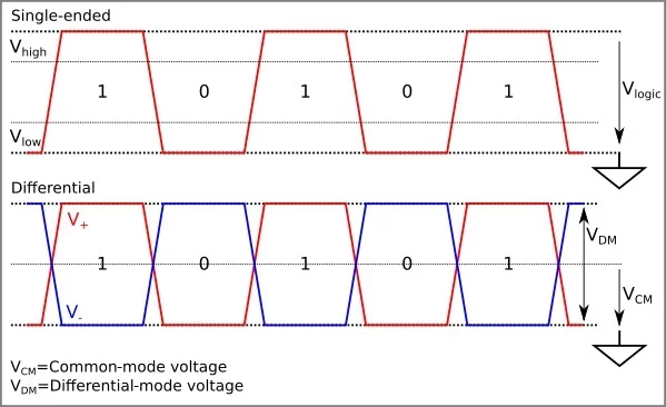
If I want to use a CML differential gate's (Ex: SY58051AU) output as the enable ECL input for an ECL counter(EX: MC100EP016A). What's the best way to connect the output to the input?

I think I need to use a Line Driver, since it's differential to single ended, but I don't think CML to ECL line drivers exist.

I thought about just connecting the positive differential output of the gate to the single-ended input of the counter and grounding the negative differential output (assuming the counter and gates are close to each other), but the voltage swing is 400 mV with a Voh = 3.28 V. Therefore, Vol = 2.88 V and the counter's Vil = 1.675 V, and 2.88 V is not less than 1.675 V. How could this connection be made?

enter image description here

Output and input levels:

enter image description here

enter image description here

\$\endgroup\$
3
  • \$\begingroup\$ Another way of asking the question: How can I go from differential CML to differential ECL and convert the ECL to single-ended ECL? If I can go directly from differeital CML to single ECL that works too. \$\endgroup\$ Commented Apr 3, 2019 at 21:00
  • \$\begingroup\$ Is your signal clock-like like the ones shown in your images? \$\endgroup\$
    – The Photon
    Commented Apr 3, 2019 at 21:09
  • \$\begingroup\$ @ThePhoton Yes, with the exception it is DC biased about 1.4 Volts \$\endgroup\$ Commented Apr 3, 2019 at 21:12

2 Answers 2

1
\$\begingroup\$

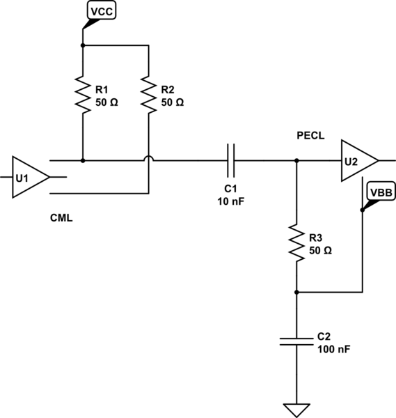
In comments you said the signal is clock-like (by which I mean switching frequently with 50% duty cycle). In this case you can simply AC-couple one of your two CML signals to the input of your PECL gate.

schematic

simulate this circuit – Schematic created using CircuitLab

If your PECL gate doesn't have a VBB pin you'll have to generate a termination voltage near the switching threshold for the PECL logic.

\$\endgroup\$
0
\$\begingroup\$

Notice there is NO SPEC for power supply rejection, despite the rather large Deterministic Jitter contribution. Given the high bandwidth, the CML gate is also vulnerable to trash induced on the input and output traces; either shield the traces, or keep high-slew-rate signals (logic of MCUs, switching supplies) well away from the CML traces.

View those 50 picosecond edges as just another version of 20GigaHertz sampler, with all the trash energy down-converted into and on top of your datastream, causing bit errors and edge jitter that degrades the bathtub dataeye.

Example: suppose there is 1pF coupling between a normal (2.5 volt/ 0.25nanoscond) MCU signal; this is 10 volts per nanosecond, or 10^10 volts per second. How much current couples thru the 1pF? I = C * dV/dT

I = 1pF * 10^10 volt/sec = 10^-12 Farad * 10^+10 volt/sec = 10^-2

I = 0.01 amps.

Now with 50 ohm termination, the dV is just Ohma Law: V = I * R.

V levelshift is 0.01 * 50 = 0.5 volts. In other words, nearly fast edges will inject a dangerous (very large charge upsets, causing lots of Deterministic Jitter) amount of current.

\$\endgroup\$

Your Answer

By clicking “Post Your Answer”, you agree to our terms of service and acknowledge you have read our privacy policy.

Not the answer you're looking for? Browse other questions tagged or ask your own question.