Overview
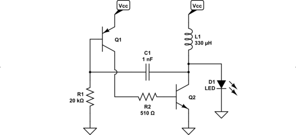
Just to get the schematic into the editor supported here and to draw it in a slightly better form for analysis:

simulate this circuit – Schematic created using CircuitLab
I've dumped the switch (implied.) I've stopped busing power around and just used a ground and \$V_\text{CC}\$ indicator, instead. This helps to focus a little better on the schematic without distracting wires which don't contribute much to understanding. But except for the switch, it is the exact same schematic as you provided.
We can make some assumptions, to start, and if they hold up well after some thought then we can consider those assumptions confirmed.
Operation
\$R_1\$ initially pulls down on \$Q_1\$'s base and turns it fully on. This also means that \$Q_1\$'s collector pulls upward on \$R_2\$ and turns \$Q_2\$ fully on, too. This then applies the full \$V_\text{CC}\$ across \$L_1\$ (less a little \$V_{\text{CE}2_\text{SAT}}\$ required for \$Q_2\$.)
With an applied voltage across ideal inductor \$L_1\$, the current in \$L_1\$ will rise according to the usual equation of \$\frac{\text{d}I_L}{\text{d}t}=\frac{V_\text{CC}-V_{\text{CE}2_\text{SAT}}}{L_1}\approx 4.2\frac{\text{mA}}{\mu\text{s}}\$. Without something happening to stop this process, it would continue forever and the current would simply increase. But the current cannot increase forever. Something is going to change, instead.
The only two possibilities are:
- \$Q_2\$ coming out of saturation because the base recombination current isn't sufficient to keep ratcheting up the collector current forever; or else,
- The core material used in making \$L_1\$ goes into saturation and the effective inductance rapidly drops (the dynamic inductance at that point starts to act as though the inductor were an air-core) and therefore the rate of current rise dramatically increases.
Either way, what changes is that \$Q_2\$ becomes recombination-current starved and it exhausts the ability of its \$\beta\$ to keep its collector pulled close to its emitter. (This moment takes place at some \$\beta\$ near its nominal active mode value, but just slightly less.)
Once \$Q_2\$ enters active mode (because of insufficient recombination current), its collector voltage rises upward (in an attempt, so to speak, to reduce its collector current to something it can handle.) But with the collector voltage rising now and therefore lifting the right side of \$C_1\$ upward, this means also that the left side of \$C_1\$ is also rising upward in voltage. But this means reducing the magnitude of \$V_{\text{BE}1}\$ and that means reducing the collector current of \$Q_1\$. But that means less recombination base current for \$Q_2\$, which is already starving as it is. So \$Q_2\$ responds by letting go still further on its collector -- with the collector voltage now rising even higher.
Together, and this happens quickly, both BJTs find themselves turned off.
Once both BJTs are fully off, \$L_1\$ is left with no choice. It must maintain its current and direction until it can get the time it needs to discharge its stored energy and let its current decline down to zero. In order for the current in \$L_1\$ to decline, the sign of \$\frac{\text{d}I_L}{\text{d}t}\$ must change. For that sign to change, the voltage across \$L_1\$ must also change sign. So the inductor responds to \$Q_2\$ turning off by suddenly reversing the voltage across itself. This means the \$Q_2\$ collector suddenly finds itself above the value of \$V_\text{CC}\$. In fact, the inductor won't stop increasing the magnitude of its reversed voltage until the current flowing through it can continue as before. Since the LED itself won't "turn on" enough to handle that current until some necessary voltage is reached, the inductor almost instantly reaches whatever voltage is needed so that the LED will conduct that peak current.
Once this is achieved, \$L_1\$ drives its current through the LED as it also declines its current towards zero.
When (and if -- as this depends on circuit design) \$L_1\$ finishes discharging its stored magnetic energy and its current reaches zero, the collector of \$Q_2\$ suddenly drops towards \$V_\text{CC}\$. This also causes the left side voltage of \$C_1\$ to suddenly drop by the same amount. (Meanwhile, \$C_1\$ is also being pulled downward by \$R_1\$ and is recharging, appropriately.) At some point in time, the left side of \$C_1\$ is low enough that \$Q_1\$ can turn back on and start supplying base recombination current to \$Q_2\$. \$Q_2\$'s collector responds by being pulled back down and this fact pulls down still more on the right side of \$C_1\$, causing the left side of \$C_1\$ to go still lower, causing \$Q_1\$ to turn on even harder than before. That supplies more base current to \$Q_2\$. Etc.
And the whole system turns fully back on and the cycle repeats.
A Design
Let's do a design. We'll assume discontinuous mode operation.
Suppose \$V_\text{CC}\$ is \$1.5\:\text{V}\$. Suppose the LED's simplified model is \$V_\text{FWD}=3.2\:\text{V}\$ and \$R_\text{ON}=2\:\Omega\$ and that the datasheet tells us that we should not exceed a pulsed \$100\:\text{mA}\$ (pulse period is \$\le 100\:\mu\text{s}\$.) Let's choose a peak current in \$L_1\$ of \$80\:\text{mA}\$. (The collector current in \$Q_2\$ also then peaks at this value.)
Given the estimated rate computed above of \$4.2\frac{\text{mA}}{\mu\text{s}}\$, we know that the on period should be about \$\approx 19\:\mu\text{s}\$. Let's round that to \$t_\text{on}=20\:\mu\text{s}\$ (parts vary too much to be more precise.)
The LED voltage will peak at \$3.2\:\text{V}+2\:\Omega\cdot 80\:\text{mA}=3.36\:\text{V}\$ so the average across the LED will be about \$3.3\:\text{V}\$. When off, the voltage across \$L_1\$ will be the difference or about \$1.8\:\text{V}\$. So the off time required is at least \$\frac{330\:\mu\text{H}\,\cdot\, 80\:\text{mA}}{1.8\:\text{V}}\$. Let's round this to \$t_\text{off}=15\:\mu\text{s}\$.
So if we really do get a peak of \$80\:\text{mA}\$ in the LED, then we should be operating at a frequency of about \$\frac{1}{20\:\mu\text{s}+15\:\mu\text{s}}\approx 28\:\text{kHz}\$. (However, the actual peak achieved will directly impact this frequency.)
Recall that \$Q_2\$ becomes recombination-current starved when \$\beta\$ is getting near to its nominal active mode value. A typical 2N2222A BJT has a nominal \$\beta=200\$ (they vary one from another, though.) Let's use \$\beta_2=120\$ as the transitioning trigger point. This means the base current needs to be capped at \$\frac{80\:\text{mA}}{120}\approx 670\:\mu\text{A}\$.
Let's also assume \$V_{\text{CE}_\text{SAT}}=100\:\text{mV}\$ for both BJTs and \$V_\text{BE}=700\:\text{mV}\$ also for both BJTs. So \$R_2=\frac{1.5\:\text{V}-100\:\text{mV}-700\:\text{mV}}{670\:\mu\text{A}}=1045\:\Omega\$. Given this isn't a precision process, round that to either \$R_2=1\:\text{k}\Omega\$ or \$R_2=1.2\:\text{k}\Omega\$.
The moment \$Q_1\$ even starts to move out of saturation, the whole process triggers anyway, so we need to use a value of \$10\le \beta_1\le 30\$ to account for its behavior. (Observe only the \$\beta_1\$ required for a fully saturated condition for \$Q_1\$.) Let's use \$\beta_1=20\$. This means that \$R_1=\frac{1.5\:\text{V}-700\:\text{mV}}{\frac{670\:\mu\text{A}}{20}=33.5\:\mu\text{A}}\approx 23.9\:\text{k}\Omega\$. Since I chose \$\beta_1=20\$, it is probably safer to reduce the resistor value to the standard value of \$R_1=22\:\text{k}\Omega\$.
What about \$C_1\$? It provides a "boost" for turning \$Q_1\$ on and off. But the main purpose is to make sure that the timing period is long enough so that \$L_1\$ can completely discharge. If \$C_1\$ is too small, it will still oscillate but the inductor will no longer operate in discontinuous mode. So it must be large enough. \$C_1\$ doesn't control the BJT on timing, but if it is large enough it does affect the off timing due to its interaction with \$R_1\$.
In this circuit, once \$L_1\$ is discharged the right side of \$C_1\$ will be at \$V_\text{CC}\$ and the left side will be about \$V_\text{CC}-V_{\text{CE}2_\text{SAT}}-V_{\text{BE}1}\approx 500\:\text{mV}\$ above \$V_\text{CC}\$. This has to drop to at least \$500\:\text{mV}\$ below \$V_\text{CC}\$.
Let's set \$f=10\:\text{kHz}\$ or \$t_\text{cycle}=100\:\mu\text{s}\$. Then \$C_1=\frac{t_\text{cycle}-t_\text{on}-t_\text{off}}{-R_1\cdot\operatorname{ln}\left(\frac12\right)}\approx 4.3\:\text{nF}\$. Just call it \$C_1=4.7\:\text{nF}\$.
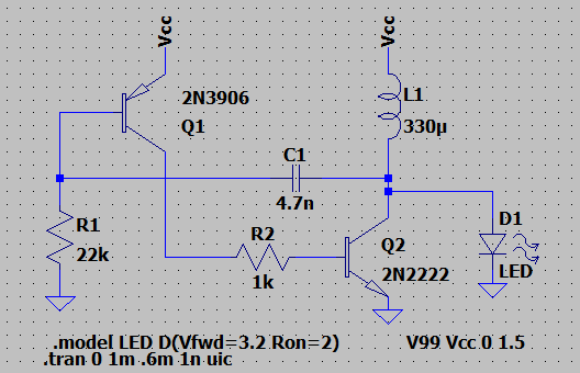
So the resulting circuit is:

simulate this circuit
The above schematic in LTspice is:

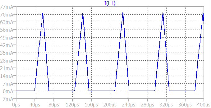
The resulting inductor current waveform is:

The resulting frequency is about \$11.7\:\text{kHz}\$. Not too far from where I targeted using simplified equations and rounding to standard valued components. And the current peaks are close enough, too.
(A more detailed analysis would require more math that I wanted to avoid.)
Footnote regarding direction of current in LTspice devices
Note: You mentioned reading a negative current and I need to point out
that you should be aware that LTspice treats each two-terminal device
as having two nodes: an entry node called "1" and an exit node called
"2". These "netlist" numbers are internal and you don't normally see
them. But LTspice does see them. When you hover over the device, there
will be a little arrow telling you which way LTspice "sees" the
current flowing. If the conventional current does flow in that
direction, it reports it as positive. If not, it reports it as
negative. If you don't like what it is reporting, you can grab the
part and reverse its direction using the "ctrl-E" keystroke and then
put the part back down into the schematic, again. It's no more serious
than that.


