0
\$\begingroup\$

General question. I see a lot of two stage amplifiers with a diff pair input and a cs second stage. In IC design these two stages are always directly coupled ie. the dc bias of the second stage is fed directly from the output of the first.

The question is then how does one properly bias the second stage? The usual method of having a current mirror acting as a current source works great at typical; however over PVT either the CS fet or the mirror fet will go into the triode region.

I see it as a two high impedance sources fighting each other. Is there a way to get around this?

Edit: For instance M8 and M7. M8 is the input device to the second stage and M7 is the mirror biased transistor.

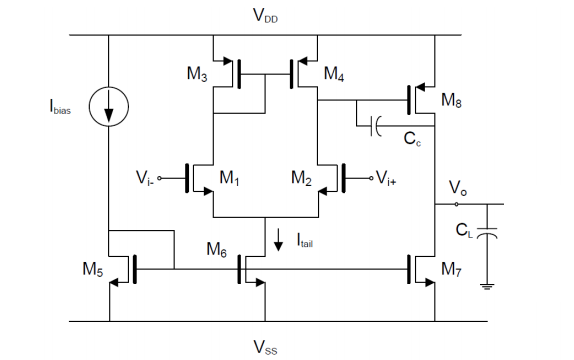
enter image description here

\$\endgroup\$
6
  • \$\begingroup\$ Can you include a schematic of the circuit you're asking about. I probably understand what you are talking about, but details matter. \$\endgroup\$
    – The Photon
    Commented Jun 17, 2019 at 16:22
  • \$\begingroup\$ I see it as having lots of current available to yank a load up or down. That also makes rise time and fall time similar. \$\endgroup\$
    – glen_geek
    Commented Jun 17, 2019 at 16:24
  • \$\begingroup\$ @glen_geek I agree, but in an amp isn't it desirable to have both devices in sat? I don't think the intent is to yank the load in this case? \$\endgroup\$
    – Char
    Commented Jun 17, 2019 at 16:31
  • \$\begingroup\$ @ThePhoton Added an img. I'm referring to M8 and M7. Thanks \$\endgroup\$
    – Char
    Commented Jun 17, 2019 at 16:32
  • \$\begingroup\$ Are you asking this as part of doing a homework problem or design project? If you increase Vdd-Vss you would not run into this problem. But maybe you were asked to design for a fairly low supply voltage as a challenge? \$\endgroup\$
    – The Photon
    Commented Jun 17, 2019 at 16:42

1 Answer 1

2
\$\begingroup\$

You're correct in spotting that that biasing M8 is indeed "tricky".

To bias M8 at the current provided by M7 the only real option is to use feedback.

I can for example use this circuit as a buffer (1x amplifier) by connecting the Vi- input directly to the output Vo.

Let's check that that is indeed negative feedback: if Vi- goes up in voltage, Id(M1) increases, Id(M4) increases so the base of M8 is pulled up and M8 will push less current into the output so Vo will drop. This drop of Vo counteracts against the rise at Vi- (with which I started) so indeed, this is negative feedback.

The feedback will force the circuit in such a state that the Vgs of M8 is such that Vo will follow Vi+.

Without feedback it is "impossible" to control M8 properly, there is so much gain at the gate of M8 that Vgs of M8 is either large or near zero. Then basically the circuit acts as a comparator.

\$\endgroup\$
3
  • \$\begingroup\$ Thanks. That is what confuses me. In the textbooks these are always shown in open loop without any feedback. So to confirm, even if the inputs are perfectly balanced, you would still need some sort of FB to make it work? \$\endgroup\$
    – Char
    Commented Jun 17, 2019 at 16:52
  • \$\begingroup\$ you would still need some sort of FB to make it work? In the real world where devices aren't 100% identical: yes you do need feedback. Only in the ideal world of a simulator (and when not using Monte Carlo analysis to simulate device mismatch) could you apply a certain input voltage that would bias M8 properly. If you ever see someone doing that you will know that person does not have much design experience as that would be totally unrealistic. In the real world only feedback will solve this. \$\endgroup\$ Commented Jun 17, 2019 at 17:04
  • \$\begingroup\$ Got it. Thanks for the help. \$\endgroup\$
    – Char
    Commented Jun 17, 2019 at 17:08

Your Answer

By clicking “Post Your Answer”, you agree to our terms of service and acknowledge you have read our privacy policy.

Not the answer you're looking for? Browse other questions tagged or ask your own question.