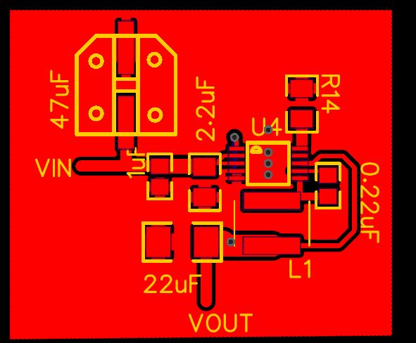
Most examples I find are for buck converters on a PCB of their own with massive traces. I want to make sure this layout is fine with the planes I'm using(both top and bottom copper pour layers are GND). I'm using a low output buck converter on a uC board I'm developing. The board will have USB to UART interface, uC, and 900 MHz radio. Total current draw is expected to be 70-100mAh, supply voltage to the board will be 12-30V. I'll leave out all these parts and just focus on the buck and buck components:
Buck: LT3970EMS-5#PBF (350mAh output max, 600Khz frequency). Inductor: ASPIAIG-S4035. R14 is just choosing frequency. Cap values are on layout. 1uF, 2.2uF, 47uF are Cin. 22uF is Cout.
All are ceramic except the 47uF. It's aluminum obviously. I have this because of what the datasheet says about capacitor transients when this device is powered from a power supply.
The data sheet has a PCB layout guideline that I found confusing. I left the Vin and Vout traces stubbed off as this hasn't been integrated into the circuit yet. I've included a close up on the pins so you guys can see the pin names. Thanks!


