5
\$\begingroup\$

I'm tweaking the design of my usb-audio device to pass the usb high speed eye pattern test. Due to the positioning of key components, the design features quite long d- d+ traces, 139mm (5.47") to be exact. In a previous iteration of the PCB, I just routed a differential trace on the default settings and got the usb funtion to work just fine. But, the length seems pushing it to meet usb compliance. That's why I want to match the impedance as best as possible while keeping transmitted and rf noise to a minimum to keep the analog part quiet.

The pcb is a 4 layer board, the part where the traces are running looks like this:
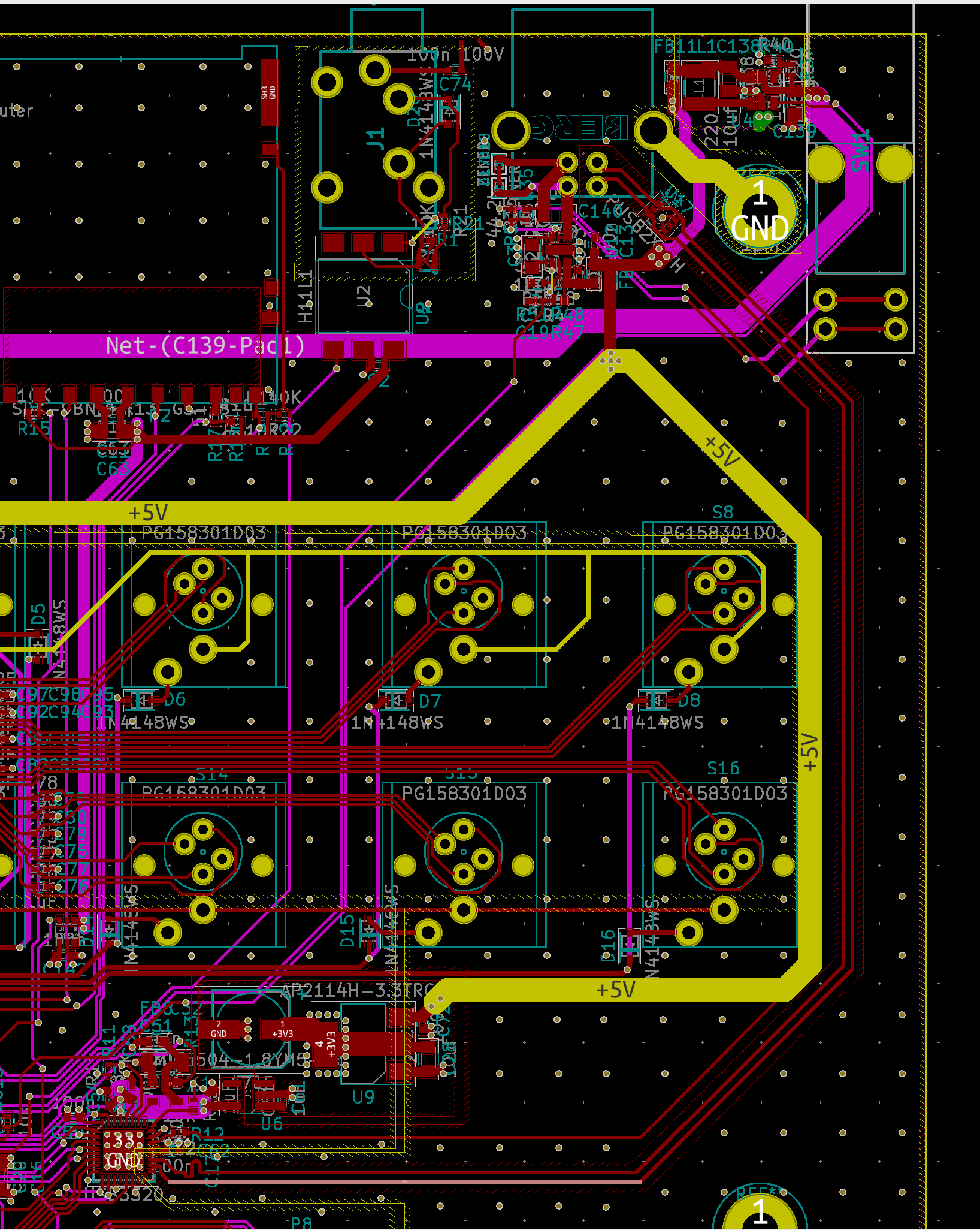
usb traces The d- d+ traces are the red ones running around the yellow +5v power trace, to the usb PHY (USB3320).

I have a few options:

  1. The option pictured below: route the traces as microstrip on the top layer (red) with a ground fill on the layer below it (yellow). This has the advantage of not having to use any vias near the PHY and the tvs-diodes near the connector. Another advantage is that, with my board-house's stackup, this option matches the 90 ohms impedance the best. The disadvantage is the wierd plane "stick-out" needed to ensure the traces reach the phy without interruption in the ground plane below. I'm not quite sure what the effect of this is. (The yellow plane surrounding the "stick-out" is 3.3v, changing that would be a lot of work.) Also, my guess is that a microstrip radiates more than a stripline.
  2. Route the traces as microsrip on the bottom layer (green). This has the advantage of having a continuous ground plance (pink, invisible) above it. Disadvantage: I'd need introduce two sets of vias if I were to keep all components on top.
  3. Stripline. Less radiated rf(?). But also again vias, and not able to achieve 90 ohms diff / 45 ohms single ended spot on with the existing stack-up (but within 5% tolerance).

Which option would you think is best?

\$\endgroup\$
6
  • \$\begingroup\$ My opinion is that an option with zero vias is best for high speed data. Vias induce unknown impedance shifts making a carefully crafted layout unpredictable. \$\endgroup\$
    – user105652
    Commented Jul 4, 2019 at 1:29
  • \$\begingroup\$ Vias induce known ESL of about 0.5 to 1nH depending geometry and a SRF well above USB2 BW, But it is not clear how 90 Ohms was computed with track to gnd on sample layer and gnd plane and adjacent track. If OK, then I see no issues with adjacent gnd plane. If no gnd pour on top layer , do that and recompute. did you measure eye margins or it just worked? And with what cable length , max? \$\endgroup\$
    – D.A.S.
    Commented Jul 4, 2019 at 1:34
  • \$\begingroup\$ Are you planning elect. Test for microstrips? At board shop? Dk tolerances must be factored then for worst case. this is all easily modelled on Falstad jitter with Symbol.exe impedance Calc. If you model all,tolerance stack ups. \$\endgroup\$
    – D.A.S.
    Commented Jul 4, 2019 at 1:40
  • \$\begingroup\$ The previous board powers and functions as usb-device just fine, albeit without eye testing. Though I haven't tried it with the max specified cable length. For the upcoming current iteration I'd like to be as close to the specified impedance as possible. The top layer does have ground pour, but has a 0.7mm keepout to the diff. traces. The impedance for the top layer traces has been calculated with saturn pcb, but it doesn't let me calculate the effect of the ground fill on the same layer. I assume the transmission line somwhat turns into a differential coplanar waveguide at that point. \$\endgroup\$ Commented Jul 4, 2019 at 10:48
  • \$\begingroup\$ 5-6" of board trace is not something of very uncommon, most PC mainboards deal with this. Why don't you post your failing eye diagram, so a better judgment can be made about why it is failing? \$\endgroup\$ Commented Jul 4, 2019 at 15:45

2 Answers 2

2
\$\begingroup\$

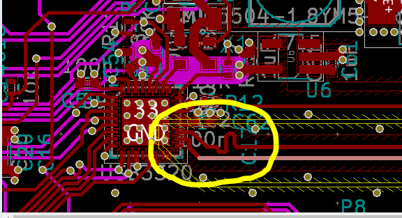
Your tracing options won't make things any better if the board has high dielectric loss. First you need to remove all the nonsense like shown below:

enter image description here

This serpentine doesn't do any good. Make the traces as straight as possible, no wiggles. 10ps delay due to length difference won't make any noticeable change in the signal. If anything, do the length compensation at the connector, so the trace would remain balanced along your board if your concern is about RF interference. In fact, USB HS emits mostly at 480 and 960 MHz, which is quite outside the audio range.

Second, use L2 as ground reference. Do your power distribution in L3 in splits. Your board's component density is not that high for not be able to do proper layer stackup and get proper power distribution from inner layers. Some parts of L2 can be used too if necessary, just make sure you have 4-5mm of contiguous plane beneath you HS differential traces.

Third, if you still see some loss of amplitude, use USB3320 Vendor Registers and boost TX strength in Reg. 0x31.

\$\endgroup\$
2
  • \$\begingroup\$ Good points you brought up Ale... \$\endgroup\$
    – user105652
    Commented Jul 5, 2019 at 6:33
  • \$\begingroup\$ Thanks, very good points indeed. Switching L2 and L3 around proved easier than I thought. \$\endgroup\$ Commented Jul 9, 2019 at 18:51
0
\$\begingroup\$

You can use either type of routing for USB, stripline or microstrip, or even a combination if you absolutely had to (best to avoid however.) For each routing type you adjust the trace width and spacing as needed to achieve the correct single-ended and differential impedance. That said, microstrip is marginally easier to deal with to meet the correct impedance since the trace will be fatter.

You have buried ground (presumably on L3). So the microstrip routing you show on your outer layer is perfectly ok and should give good results. Stitch that plane to L3 however.

You could also via the USB pair down to L4 as you propose, then via them back up to L1. That’s not ideal as it Introduces time domain discontinuities, but it would probably still work.

Why not just make L2 your ground plane?

\$\endgroup\$
1
  • \$\begingroup\$ It's a bit tricky to tell, but the microstrip on top as pictured has L2 (yellow) as ground plane running below it. Where the fat yellow trace reaches the regulator on the bottom, the plane ends. Left of that, the plane becomes a power plane for 3v3. To make sure the traces reach the PHY with uninterrupted copper beneath them, the ground plane protudes into the 3v3 plane and actually connects to the thermal vias under the PHY. L3 is signal with a ground pour, L4 is almost entirely ground as well. All the ground planes are stiches together. \$\endgroup\$ Commented Jul 4, 2019 at 10:40

Your Answer

By clicking “Post Your Answer”, you agree to our terms of service and acknowledge you have read our privacy policy.

Not the answer you're looking for? Browse other questions tagged or ask your own question.