7
\$\begingroup\$

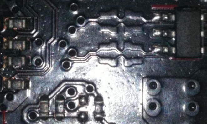
picture of oddly shaped traces, with other components for scale

photo of board with additional context

I was taking a look at my motherboard, and I noticed the above traces on the USB 3.0 ports. A bit of prior research:

  • The C34WH IC is probably a SN74LVC2G34 Dual Buffer Gate.
  • Unclear what chip the top two ICs are, but the markings likely read 1188J.

What is the purpose of making these traces like this?

How is the appropriate shape of the traces calculated?

\$\endgroup\$
4
  • \$\begingroup\$ I'm not quite able to make sense of them: If they were impedance matching elements, then the chip to the right wouldn't be in a leaded package, because the thickness and width of the pins would probably have more influence on the HF properties than these small symmetrical structures. \$\endgroup\$ Commented Jul 20, 2019 at 20:39
  • \$\begingroup\$ Are those data lines? \$\endgroup\$
    – MadHatter
    Commented Jul 20, 2019 at 23:34
  • 1
    \$\begingroup\$ @MadHatter I didn't trace them all the way to the port, but I'd say that it is likely that they are data lines. They are very thin, and they pass through some kind of transceiver. \$\endgroup\$
    – flaviut
    Commented Jul 21, 2019 at 0:05
  • 4
    \$\begingroup\$ It's some kind of differential filter, and you'd probably have to have a really nice FEM package to design it. The wider traces would give you less inductance followed by more inductance (with the thin trace) and then less again. The capacitance would also go up, then down then up again. Pretty much witchcraft \$\endgroup\$
    – Voltage Spike
    Commented Jul 21, 2019 at 1:50

1 Answer 1

6
\$\begingroup\$

My best hypothesis is that these are common mode noise filters

The thick regions in each section represent capacitors, most likely to the ground plane of the pcb.

The half loop pattern in the middle would seem to be a common mode choke for really high frequency noise. USB 3.0 runs in the gigahertz so this seems about right. The common mode choke is a classic approach to reducing noise common to both sides of a balanced line while having little effect on the differential signal that is desired.

Together these form a CLC filter called a balanced PI filter network.

\$\endgroup\$

Your Answer

By clicking “Post Your Answer”, you agree to our terms of service and acknowledge you have read our privacy policy.

Not the answer you're looking for? Browse other questions tagged or ask your own question.