4
\$\begingroup\$

I get it that voltage drop across active loads are less compared to passive loads and at the same time they offer high small signal impedance thereby increasing gain.

I cannot understand why DC voltage drop across them is lower compared to passive loads like resistors.

In the book "Fundamentals of Microelectronics" by Prof. Behzad Razavi, it's written that active loads don't follow Ohm's law like resistors. Okay I agree but still I don't get why the DC voltage drop across an active load will be lower.

\$\endgroup\$

5 Answers 5

4
\$\begingroup\$

Active loads are used because transistors are cheaper and easier to make on a silicon die than resistors are. Therefore, you find active loads more in integrated circuits while discrete circuits tend to use resistors more for simplicity (and less availability of matched transistors).

I cannot understand why dc voltage drop across them is lesser compared to passive loads like resistor. I don't get why the dc voltage drop across a active load will be lesser.

The wording and emphasis is strange. I think he's trying to say that if you use a transistors instead of a resistor for a current source, then you don't need such a high voltage rail to approach the ideal current source.

An ideal current source has infinite output resistance (since any changes in load impedance should not affect the current output) which means you need an infinite voltage rail to push current through it.

If you try and implement this in practice, it means you use a very large resistor which necessitates the use of a high voltage rail. The more you increase your resistance to approach the ideal current source, the more you also need to increase your voltage rail.

I guess the DC voltage drop across this resistor is what he is referring to when he says that the DC voltage drop. He's omitting the part where there is a higher voltage rail present which is supplying this higher voltage drop.

If you use transistor current source, then you can get a really high output resistance (i.e. you can get something that approaches the ideal current source) without using such a high voltage rail, which technically means that your voltage drop will be lower. But I wouldn't really emphasize the fact that the DC voltage drop is lower...that's a bit confusing. I agree.

\$\endgroup\$
2
\$\begingroup\$

If you use a resistor as a load, then its slope resistance (change in voltage drop / change in current through) is equal to its resistance. If it's being used to bias an amplifier, then its voltage drop is given by the bias current times the resistance. If you want a higher slope resistance, then you have to suffer a corresponding higher voltage drop at any given bias current.

If you use an active load, then it's possible to design both the voltage drop and the slope resistance separately. Consider a simple transistor current source. It can maintain a very high slope resistance, right down to a voltage drop of the volt or two needed to bias itself.

\$\endgroup\$
2
  • \$\begingroup\$ Can you tell me how do you design such an active load as transistor? I mean what are the design parameters to keep in mind . Like say how will I control what voltage drops across an active load \$\endgroup\$ Commented Jul 31, 2019 at 15:33
  • \$\begingroup\$ In a circuit like this go down to section 2.3.1.2 R2 and DZ1 determine the magnitude of the bias current it provides to the load, but the output impedance of Q1 is very high, orders of magnitude larger than R2. It stays that way for VCEs between about 1v, and a max voltage limited by the transistor heat dissipation. \$\endgroup\$
    – Neil_UK
    Commented Jul 31, 2019 at 19:10
2
\$\begingroup\$

Sometimes an image is worth a thousand words. Suppose you are interested in a voltage amplifier (or a transimpedance amplifier for what is worth) where your transistor is required to achieve a given swing on its Vce voltage. (a simple CE stage would do that)

You can use a small Rc and achieve such a swing at the expense of a large variation in Vbe or Ib (we are not interested in the surrounding circuitry, let's focus on the output characteristics of the transistor only). Like so:
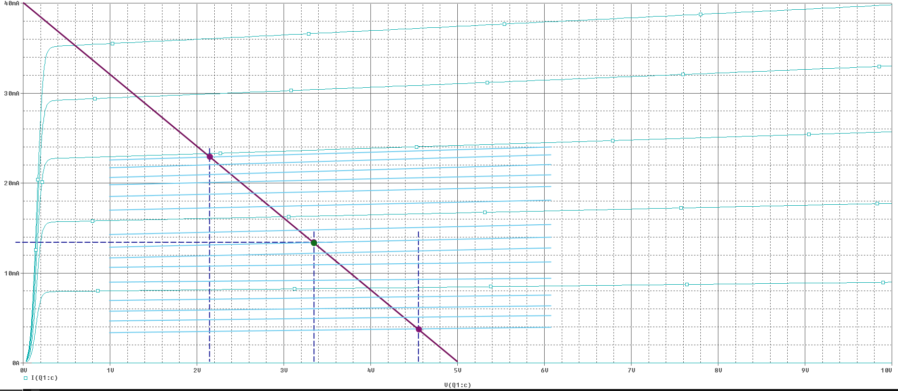
Small RC

The interesection with the Vce axis is your power supply voltage Vcc. You might want to ramp up the amplification by using a bigger RC. But if you want to keep the same quiescent point (it's useful to compare the different solutions) you will have to increase your supply voltage. This is evident from the following image:
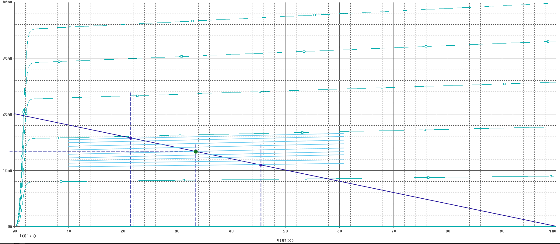
Big RC

See how the same swing in Vce requires a smaller swing in Ib (and thus Vbe)? This will translate in an increased amplification. (Yes, you can also make the Vce swing bigger for the same input swing, but the graphs are tidier this way). So, let's make Rc really big:
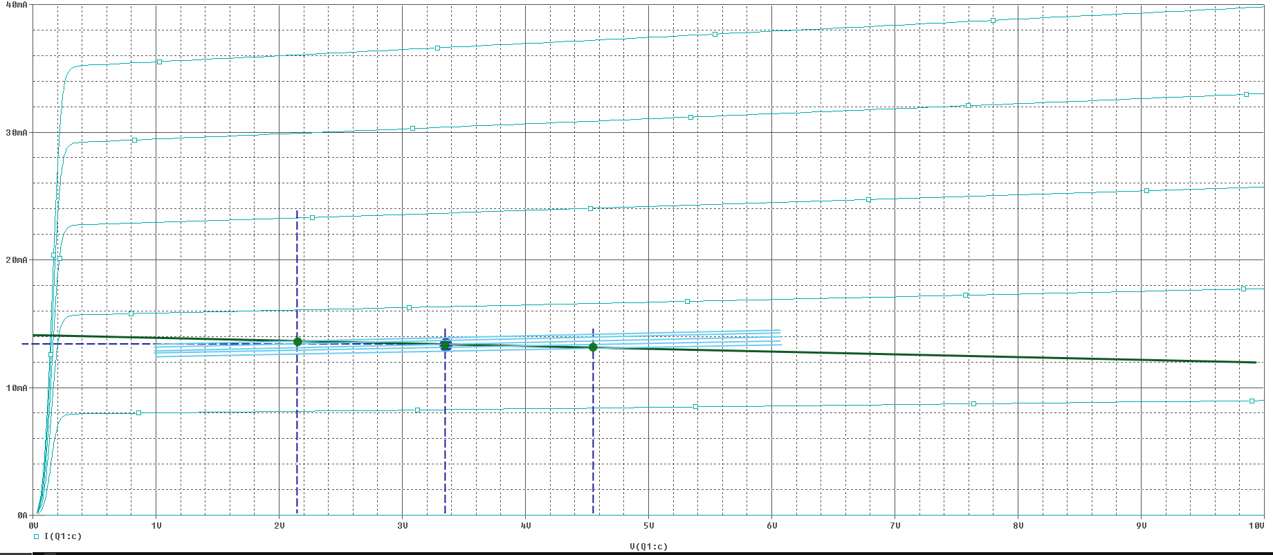
Huge RC

With great resistors come great power supplybilities. This is not always feasible for several reasons, so wouldn't it be nice to have the same slope of the load lin--- no, the load curve, but not having it to go way over the transistor limits on the Vce axis? All we need to to is... bend it. So a straight line wouldn't work, and this rules out linear components such as simple resistors. But nonlinear devices like transistors are still good. And in fact, by using a transistor as load we get to use its output characteristic with that steep vertical part near saturation. Like this:
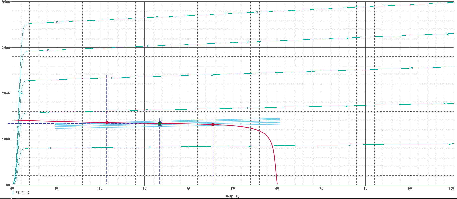
Active load

The curve is mirrored and translated by Vcc, like we did with straigh line of a resistor, but the nonlinearity helps in keeping the supply voltage at a lower value.

\$\endgroup\$
1
\$\begingroup\$

Perhaps a simple example with real numbers may help to explain the difference:

  • Lets assume that for high gain we need a dynamical collector resistance of rc=20k.

  • In case of an ohmic (passive) part we have rc=Rc=50k with a DC drop of 20V for Ic=1mA. In many cases, this is unacceptable (Large supply voltage).

  • Using a BJT as an active load it is not a problem to realize rc=20k (dynamic resistance), but at the same time we can have a DC drop across the load resistor of Vce=5V or so...

\$\endgroup\$
0
\$\begingroup\$

FET's are voltage controlled Resistors according to (Vgs-Vt) over the range of Vds to sink current from Nch Enhancement mode FET's when used as open-drain loads to a power source. The resulting Rds is not inverse linear with gate voltage but can be made linear with feedback.

BJT's are exponential Vbe controlled current sinks or with a base resistor, Current controlled current sinks except when hFE reduces to 10% of hFE near max current starting typically below Vce<2V at max hFE. Without current sensing these are non-linear in this region of saturation, yet fairly linear current down to Early effect leakage currents.

Both FET's and BJT's are excellent active linear loads for performing this task when used with calibrated gm and may be used as fixed Resistors in FET's or constant current in both with current feedback when calibrated due to component tolerances.

Current sensing eliminates the need for calibration as it is then based on resistor tolerances which are orders of magnitude less in error than gm or hFE.

\$\endgroup\$

Your Answer

By clicking “Post Your Answer”, you agree to our terms of service and acknowledge you have read our privacy policy.

Not the answer you're looking for? Browse other questions tagged or ask your own question.