2
\$\begingroup\$

I'm trying to understand how the auto bi-directional voltage translators work.

Background:

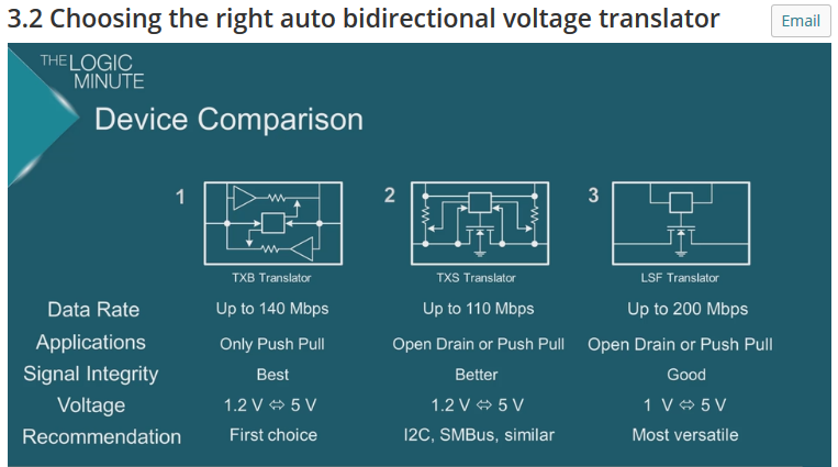
I have to choose a part that can translate signals in both directions between 1.8 and 3.3 volts. However, there is a wide selection of components that does this and perhaps anyone would work. But I want to understand how they work, so I was watching this TI video where they use at least 3 different methods with Only Push-Pull, Open-Drain and PP. Later in the video they state that Only PP (i.e. the TXB series) may not always work.

enter image description here

What are the use cases/scenarios when it would not work?

I believe that understanding the PP vs. OD, and how the bi-directional properties are determined, would help me understand what I really need. So my question is:

How does an auto bidirectional voltage translator work?


I've also looked at the following SE-EE post, but did not find it helpful in my case.

(It doesn't seem to explain how the direction is determined.)

\$\endgroup\$
1
  • \$\begingroup\$ All great answers, but I can only accept one. \$\endgroup\$
    – not2qubit
    Commented Aug 6, 2019 at 14:53

3 Answers 3

3
\$\begingroup\$

The direction is determined by the external output "overpowering" the translator output which forces the direction.

If the external output cannot drive enough current to maintain appropriate levels at the translator pin, the translator direction may not be reliably switched, perhaps only under some conditions, and bad things may ensue. Some use a one-shot that briefly, during output transitions, enables a strong output to charge external capacitance and then the output strength drops back to a few mA capability, which is easier to overpower.

For this reason, it may be best to use translators that have a direction input in some situations, and you should always carefully evaluate the requirements for all devices connected on each side of the translator.

\$\endgroup\$
2
\$\begingroup\$

PP (push-pull) means that the output provides current in both directions (sinking and sourcing). A "1" on the output will provide a positive drive voltage at the logic level, and a "0" will pull the output down near ground. This will not work with some bus circuitry such as I2C or SMBus because you cannot tie two push-pull outputs together. If you do, and one is high and the other low, they will try to drive each other resulting in high current and an undefined output.

OD (Open Drain) outputs only sink current. When the output is "0," the line is pulled down near ground, but when the output is "1," the line is high impedance, as if it was disconnected from the output circuit. Therefore, you can tie many of these types of outputs together with a "pull-up" resistor (tied to the logic voltage) to pull the logic level up to the logic "1" voltage when all of the outputs on the bus are at the "1" state. Since the outputs can only pull down, any of the outputs on the bus can safely pull the line to a logic "0" state when the other outputs are still in the "1" state. In this manner, multiple outputs can "take turns" communicating on the same bus line.

\$\endgroup\$
2
\$\begingroup\$
  • The LSF works pretty much exactly like the shifter in the linked question (because it is just a MOSFET).

    There is no mechanism to detect the direction; the LSF is a passive switch. When either side is pulled low by an external device, the transistor activates and pulls the other side low; when neither side is pulled low, the transistor is not active, and the voltages at both sides are determined by the pull-up resistors.

    The LSF does not care whether an external device actively drives the signal line high, or whether it is only due to the pull-up resistor. This allows it to be used with both push/pull and open-drain signals.

  • The TXS works like the LSF. The difference is that it has integrated pull-up resistors, and edge accelerators, but those do not affect the basic mechanism.

  • The TXB has drivers in both directions. There is no mechanism to detect the direction; both directions are always active. To allow external devices to override the voltage, the TXB drivers are deliberately made very weak.

    The TXB works only if the external drivers are stronger than its own ones, and if the external inputs have a much higher impedance that its own ones. This means that it is not possible to have normal pull-up or pull-down resistors (they would be stronger than the TXB's outputs), and that you cannot drive any load that is larger than a CMOS input.

    The TXB does not work with open-drain signals because a pull-up resistor would not be strong enough to drive a TXB input.

\$\endgroup\$
2
  • \$\begingroup\$ Can you clarify the meaning of: "you cannot drive any load that is larger than a CMOS input."? \$\endgroup\$
    – not2qubit
    Commented Aug 6, 2019 at 14:53
  • 1
    \$\begingroup\$ The TXB outputs are not rated for more than 20 µA. \$\endgroup\$
    – CL.
    Commented Aug 6, 2019 at 15:31

Your Answer

By clicking “Post Your Answer”, you agree to our terms of service and acknowledge you have read our privacy policy.

Not the answer you're looking for? Browse other questions tagged or ask your own question.