5
\$\begingroup\$

I'm designing a gate drive and I saw in a reference design this circuit, what would be the explanation for placing a capacitor between gate-source of the MOSFET (or IGBT)? I've read that a resistor is also placed likewise to prevent sudden turn ons? *Also though it says it's not mounted, I'm thinking there was a reason for placing it. Gate drive from STmicroelectronics
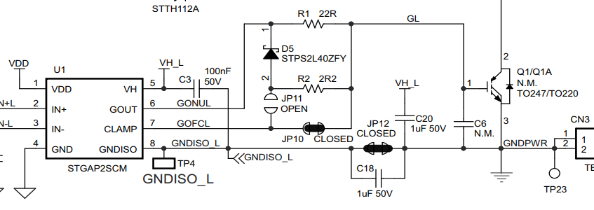
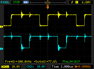
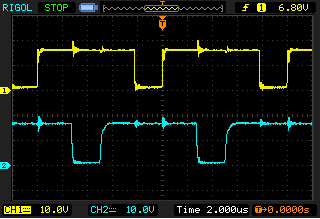
I did some test with:

  1. No capacitor
  2. 1nF capacitor
  3. 10nF capacitor

I added an idea of the schematic of what I'm testing, I'm using SiC MOSFETS, the power stage are two boost converters with common ground.

The driver ground is connected to the power ground of course.

This is what I found:
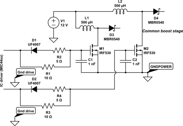
schematic

simulate this circuit – Schematic created using CircuitLab

With no capacitor

1nF capacitor[![][3]]4

10nF capacitor

I think it is highly related to the comments of Marcus Müller and the answer of JonRB.

Further explanation of this is appreciated.

Thanks

\$\endgroup\$
6
  • 1
    \$\begingroup\$ note that the footprint of a capacitor and a resistor are typically identical. I could imagine it being for overshoot dampening reasons, but I don't see how these would be problematic here, either. \$\endgroup\$ Commented Aug 11, 2019 at 19:45
  • \$\begingroup\$ That is weird. Gate capacitance is undesirable, let alone adding it externally. It's almost like they were concerned with noise affecting the gate but a gate-emitter cap is bad in so many other ways. \$\endgroup\$
    – DKNguyen
    Commented Aug 11, 2019 at 20:00
  • 1
    \$\begingroup\$ maybe the answer is that it's a reference design, and the idea is that "if you want to simulate usage of a higher GE capacitance transistor, this is where you'd put a capacitor" or something. \$\endgroup\$ Commented Aug 11, 2019 at 20:26
  • \$\begingroup\$ Can you give a link to this reference design? \$\endgroup\$
    – jusaca
    Commented Aug 11, 2019 at 20:52
  • \$\begingroup\$ st.com/resource/en/data_brief/evalstgap2scm.pdf \$\endgroup\$
    – E.pow93
    Commented Aug 11, 2019 at 22:00

3 Answers 3

3
\$\begingroup\$

This is sometimes added if a specific instance is susceptible to dv/dt turn-on (layout, lower current drive, installation). A collector-gate current, via the parasitic capacitance: Ccg flows at every switching event. If the gatedrive does not have enough drive capability to absorb this charge then the IGBT can inadvertently turn on.

By adding a capacitor in parallel with the devices Cge, this capacitor will aid in absorbing the charge at the expense of increasing the gatedrive power need

\$\endgroup\$
2
  • \$\begingroup\$ Is there any reason you would choose to increase the gate capacitance in this way instead of just throwing an RC snubber across the collector/drain and emitter/source? Or is the dV/dt turn on you describe different from what I am thinking of? \$\endgroup\$
    – DKNguyen
    Commented Aug 12, 2019 at 1:53
  • \$\begingroup\$ A snubber will slow down the switching characteristics. If the gatedrive can handle the extra power, this doesn't really change the switching speed, \$\endgroup\$
    – user16222
    Commented Aug 12, 2019 at 6:37
1
\$\begingroup\$

C6 is unusual and would usually be detrimental.
R1 is on the high side and especially so if C6 is installed.
Gate time constant = Trc_= R1 x Cg should be small wrt switching times but not very small.

Related:

Move D5 to immediately physically adjacent to Q1/Q1A - as close to the GS leads as possible.
It clips negative gate ringing peaks and takes energy out of gate oscillations.

Also add a reverse biased zener at the same location, of voltage slightly above Vdrive max.
This absorbs positive transients from eg Millar coupling from load.
Notionally only needed if load inductive (yours is) BUT always a good idea.

\$\endgroup\$
0
\$\begingroup\$

It can help you with self-turn on problems as it is explained in https://toshiba.semicon-storage.com/info/application_note_en_20180726_AKX00074.pdf?did=59473 chapter 3. It will also demand more power from the driver if you add it. Also, it can help you with your ringing as your experiment confirmed. This is because it decreases the impedance, so the Q factor during turn OFF since it increases Cgs. Here you will find an excellent explanation about the Q factor:

Calculating the pulldown resistance for a given MOSFET's gate

\$\endgroup\$

Your Answer

By clicking “Post Your Answer”, you agree to our terms of service and acknowledge you have read our privacy policy.

Not the answer you're looking for? Browse other questions tagged or ask your own question.