3
\$\begingroup\$

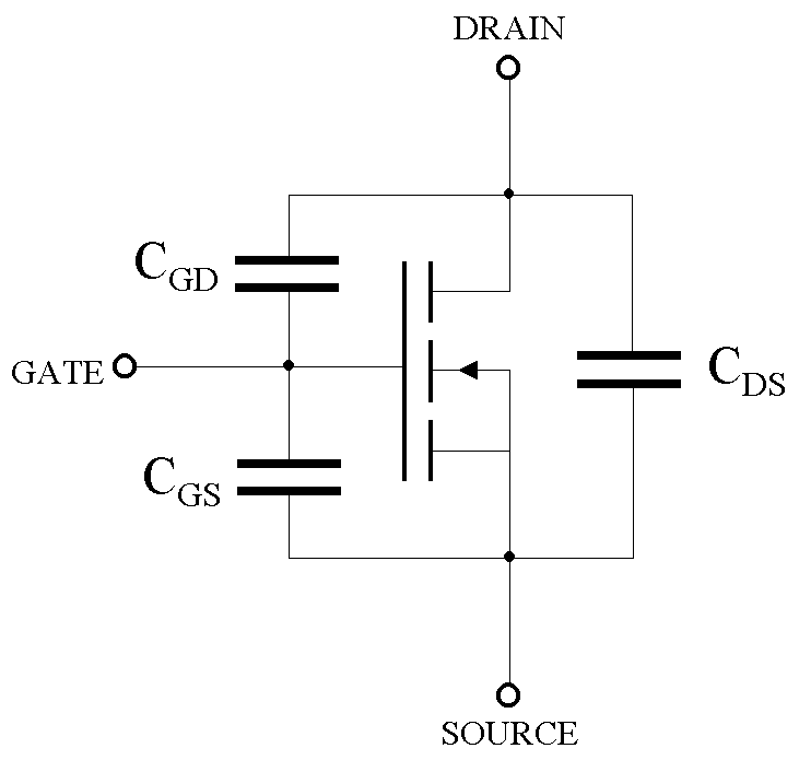
I need some explanations about the MOSFET parasitic capacitances. Precisely, what I studied is that there are those parasitic capacitances:

enter image description here

But generally in digital electronics texts I see that they are not considered (for instance let's consider a CMOS inverter): there are simply an input capacitance (between input terminal and GND) and an output capacitance (between output terminal and GND).

What is the physical cause of them (for instance we know that CGD is determined by the overlap between the gate and drain metal's etc)? Are they equivalent models of the previous capacitances (and if yes, how do we obtain them)?

\$\endgroup\$
3
  • 2
    \$\begingroup\$ I guess answer to this is all over google under "Mosfet capacitance" \$\endgroup\$
    – Mitu Raj
    Commented Aug 30, 2019 at 12:03
  • 1
    \$\begingroup\$ most datasheets will separately define them as you have drawn, when your only interested in switching a signal on or off, instead your after the "Theravin equivalent capacitance of Cgd/Cgs" to know how much charge you have to move on average. generally just called "Input Capacitance", with Cds as output capacitance. They do also change with voltage, the mismatch between them vs bias voltage is what causes charge injection in analog switches. \$\endgroup\$
    – Reroute
    Commented Aug 30, 2019 at 12:15
  • \$\begingroup\$ The drain-source will be thru the Well or thru the Substrate. The Well-Substrate capacitor is a useful charge storage element, contributing to stabilization of the VDD in a logic-oriented IC. Without local charge storage, and plenty of local well-contacts (well-ties) and substrate-contacts, you'll have VDD collapse and SHMOO_holes in the Fclock_VDD_whatpackage plot. \$\endgroup\$ Commented Aug 30, 2019 at 14:32

1 Answer 1

2
\$\begingroup\$

The parasitic capacitances in MOSFETs (Cgs, Cgd, Cds) are physical effects due to overlapping regions in the transistor structure. In digital circuits like CMOS inverters, they are often grouped into simplified input and output capacitances. For example, Cgs is associated with the input capacitance, and Cgd is part of the output capacitance. These capacitances arise from charge interactions between different transistor regions, impacting the circuit's performance. The simplified models help in understanding and designing digital circuits, especially at lower frequencies, while more accurate modeling is essential for higher frequencies or analog applications.

\$\endgroup\$

Your Answer

By clicking “Post Your Answer”, you agree to our terms of service and acknowledge you have read our privacy policy.

Not the answer you're looking for? Browse other questions tagged or ask your own question.