1
\$\begingroup\$

I'm aware the same question has been posted before, but unfortunately, it has not led me to an answer.

I have a small PCB in which I've added an LDO to convert input voltage to 3.3 V output voltage.

The LDO in using is the AP2210-3.3TRG1 (datasheet). My understanding from the datasheet is that with an input voltage of 4.3 V - 13.2 V. (4.3 V because the manufacturer recommends Vout + 1 V). I'm supplying 9 V input voltage from a battery.

My schematic is as follows:

schematic

simulate this circuit – Schematic created using CircuitLab

I'm expecting to get 3.3 V as output voltage. When I measure the output voltage, however, my multimeter reads only 0.5 V.

I've gone through the datasheet to see if I've misunderstood or missed something, but I can not manage to figure it out. There's also some stuff I do not really understand, which doesn't help.

So some concrete questions. Do I have some mistake in my schematic? Am I misunderstanding how to use this component?

I hand soldered the part on a PCB (with hot air), is it possible I overexposed it to heat?

UPDATE

Thank you all for your answers!

Some additional information:

The load is an ESP8266 (datasheet). I've measured the current at the LDO output, which is ~135 mA.

When I measure the voltage at the same spot I get 1 V now. In the original post, I reported reading 0.5 V, but I must've been mistaken since nothing has changed and now I get a solid 1 V (which is still lower than expected).

In regards to "Power Dissipation"; I get the following results (as per page 23 of the LDO datasheet):
(150°C - 25°C) / (0.135 A × 200°C/W) + 3.3 V = 7.93 V

This is a lower voltage than I'm supplying. Can this be the issue? The datasheet says:

Therefore, for good performance, please make sure that input voltage is less than ...

I'm going to find a 5V power source and see what happens!

Results I supplied ~4.8V and measure the following values at Vout:

85-90 mA

0.7-0.75 V

I also feel the LDO is getting significantly hotter now, but I've not verified that.

UPDATE

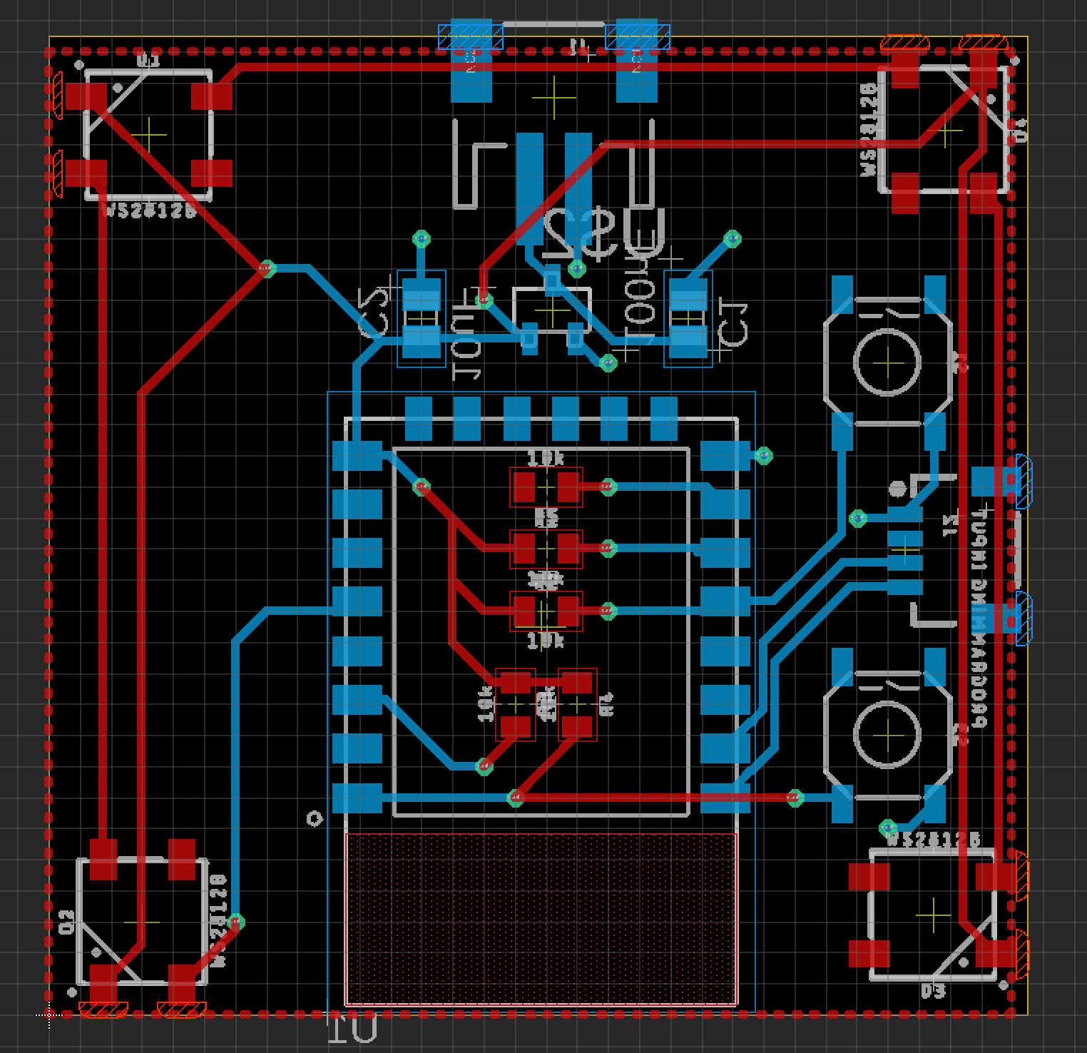
Adding a screenshot of the board design.

board design

resistors on top layer are 10k ohm resistors.

C1 is a 1 uF cap and C2 is a 2.2 uF cap.

U1 is an ESP-12F

\$\endgroup\$
7
  • \$\begingroup\$ "I hand soldered the part on a PCB (with hot air), is it possible I overexposed it to heat?" Maybe, how long did you hold the hot air on it? Did you measure the output with any load on it? \$\endgroup\$
    – serpixo
    Commented Dec 6, 2019 at 22:32
  • \$\begingroup\$ Is the voltage you report with or without a load? If with a load, how much current does the load draw? \$\endgroup\$ Commented Dec 6, 2019 at 22:32
  • \$\begingroup\$ Check to see if Page 23 of the datasheet applies to you. "Power Dissipation". Confirm you're connecting to the right pins ("1, 2, 3" which are not labeled on your schematic). \$\endgroup\$ Commented Dec 6, 2019 at 22:33
  • \$\begingroup\$ Based on what you've described, you seem to understand how the part should work. The problem must then lie within your implementation. A few things to check: What is your expected load? What is the current draw from the source? Double check pinout of package. Ohm out the output. Replace part. \$\endgroup\$
    – BEE
    Commented Dec 6, 2019 at 22:38
  • 1
    \$\begingroup\$ A picture is worth a thousand words. Post a photo of your construction. \$\endgroup\$ Commented Dec 7, 2019 at 3:51

4 Answers 4

1
\$\begingroup\$

The first thing I consider in these situations is load / power and the next is stability.

Parts with a PNP pass element (particularly earlier and less expensive parts) often require a minimum ESR in the output capacitor path for stability.

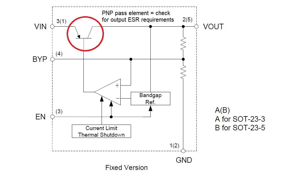
Here is the simplified schematic for your regulator:

AP2210 simplified schematic

I have added a note about what I do when I see a PNP (or any P type) pass element:

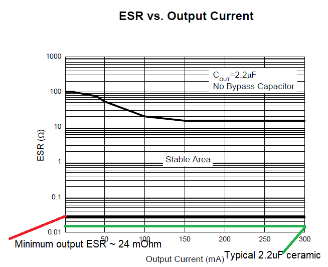
Going to page 22 of the datasheet we do indeed see a minimum ESR requirement:

AP2210 ESR band

Given the small size of the parts on your PCB, it looks like they are ceramics which typically have an ESR below the recommended minimum.

That leads me to believe the device is possibly oscillating or otherwise unstable which would render it quite hot in very short order.

\$\endgroup\$
1
  • \$\begingroup\$ So one could add a resistor (e.g., 100 milliohm) in series with the output capacitor to move the ESR into the stable region, correct? Further, it's a pity that the datasheet is silent about the stable area when a "bypass capacitor" is connected. \$\endgroup\$
    – Daniel K.
    Commented Jan 9, 2023 at 17:38
0
\$\begingroup\$

I've been soldering PCB's for years and never had a component fail due to overheating. You'll find this is the case for many others (see How to tell if chips overheat while soldering).

If you are using the SOT-23-3 version of this chip, it's pretty much a guarantee you have a goof in your setup (dry solder joint, internally disconnected wire, burned out chip) since you only have three pins to connect. There is no mistake in your schematic, so something else is going on. Try checking the current draw with no load (if it's high, your chip is blown), and double check your pin mapping and continuity.

\$\endgroup\$
1
  • \$\begingroup\$ Thank you for your answer Ocanath. I checked my pin mapping and it seems to be correct. I'm also getting continuity, so I'm assuming it's to do with my voltage supply and the load. I'm feeling quite certain now I haven't overheated the component. \$\endgroup\$
    – Jeroen
    Commented Dec 7, 2019 at 11:27
0
\$\begingroup\$

Update

Below I estimated 5.7V*109mA=600mW =Pd loss for a 3.3V*109mA = 360mW load.
We do not know the linearity of your new results but the size of the chip without a copper heatsink suggests 600mW should be derated by at least 50%.

Reduce your load, or change the design to a part with a heatsink or much higher power rating than this.

Estimating the load impedance.

0.75/90mA ~ 8 ohms
3.3V/90mA ~ 37 ohms

You can experiment lowering the input voltage if you have no linear adjustable supply source ,do an experiment and add a 10 ~30 Ohm input resistor to reduce the temp rise in the LDO.

** It appears to be a diode drop for some reason hmm**

I am leaning towards internal load short cct. and diode drop characteristic failure ESD suggestion 2)


1) Excess linear power drop?

\$\theta_{JA}=200 ~' C/W~~~~\Delta V_{IN-OUT}=5.7,~~~~ T_J=150'C,~~~ I_{max}=125_{'C_{rise}}~~/200'_{C/W}/5.7V = estimated~ 109mA ~~absolute~ maximum\$

2) Electro Over Stress (EOS) semiconductor handling environment (training/reading)

3) Excess liquid solder dwell time. ( read solder profile for IC)

\$\endgroup\$
2
  • \$\begingroup\$ Thank you for your response! From your calculation, it looks like I may be drawing too much current (~0.135mA at Vout). However, I specifically choose this LDO for its 300mA current output. Does this mean I need to change my power supply? For example, if I supply the circuit with a 5V supply: 125/200/1,7 = 368 mA absolute max? \$\endgroup\$
    – Jeroen
    Commented Dec 7, 2019 at 11:33
  • \$\begingroup\$ What is too much current (~0.135mA at Vout)?? \$\endgroup\$
    – D.A.S.
    Commented Dec 7, 2019 at 17:59
0
\$\begingroup\$

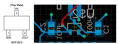
Pin2, "Vout", appears to be grounded on your pcb.

enter image description here

...and C2 is connected to Pin 1.

That's probably not what you intended.

\$\endgroup\$
1
  • \$\begingroup\$ This looks like Eagle; blue is the bottom layer so this is looking at the bottom of the package (ie, as if it's mirrored). It's correct, unless colours have been changed. \$\endgroup\$
    – awjlogan
    Commented Dec 9, 2019 at 13:37

Your Answer

By clicking “Post Your Answer”, you agree to our terms of service and acknowledge you have read our privacy policy.

Not the answer you're looking for? Browse other questions tagged or ask your own question.