My intuitive understanding of the common-mode feedback is based on the concept of dual dynamic load. As I have fabricated this descriptive name to explain the idea behind CMFB in a more figurative way, I will show you the path that I walked on to reach it. There is nothing weird in my explanations as you would think from looking at these unconventional pictures. Rather, they are based on simple electrical concepts comprehensible for everyone... and this is the power of intuitive approach.
Building a half differential pair
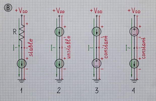
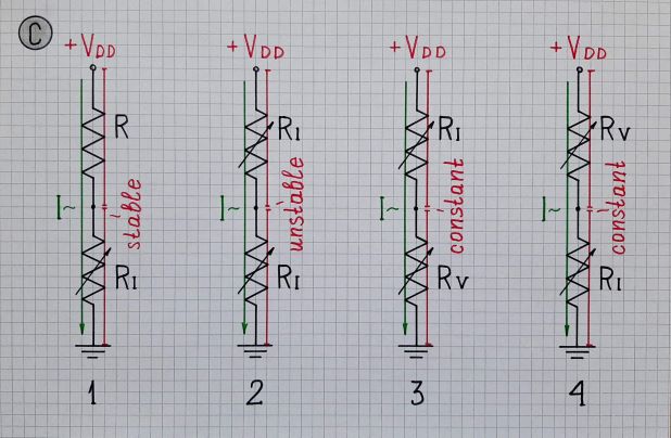
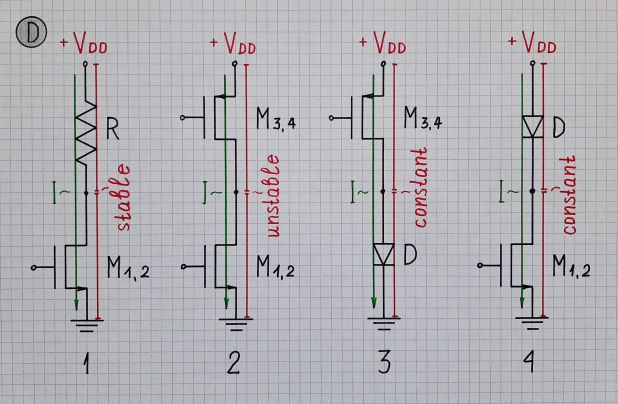
First, I will show the main idea in four consecutive conceptual pictures (marked with letters A - D). Each of them contains four versions (numbered with 1-4 in each picture). Then, each of the versions is illustrated with a separate picture (numbered with 1 - 4) with the corresponding MOSFET implementation from the Razavi's book. The series finishes with a generalized picture 5.
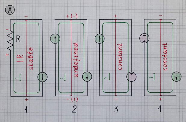
A. Interacting sources. The simplest electrical circuit possible consists of two elements - source and load. Besides passive (resistor), the load can be active (another source)... in this quite more interesting case there are two interacting sources. One of them is the "initiator" and the other responds to its impact.
The combinations between both elements can be various but let's consider only these related to our subject (five MOSFET circuits with CMFB from the Razavi's book). Note there is no ground in the picture below (it is not needed yet). The four diagrams in the picture (numbered with 1 - 4) are drawn in a form consistent with the next steps.

Current source drives resistive load (1). In this arrangement, constant current flows through constant resistance and creates a voltage drop across it. This voltage is stable since it is well defined by Ohm's law and it does not change by itself.
Its magnitude can be significant.
Current source drives current source (2). Here, two equivalent current sources are connected in series (one current source serves as a dynamic load of the other source). The voltage across them is unstable and can be easily changed by itself. As above, its magnitude can be significant.
Voltage source drives current source (3). This is the perfect combination between two sources since the voltage source sets the voltage across them and the current source sets the current through them. The voltage is stable and constant... and limited by the voltage source.
Current source drives voltage source (4). This is the same perfect combination as above. It is inserted here for completeness (in the next implementations it will be used).
B. Interacting sources and sinks. Electronic circuits are supplied by a power supply which negative terminal (usually) serves as a ground. So the pairs of sources above are "stretched" between the supply rails - one of the sources in each pair is connected to the positive supply rail and acts as a source; the other is connected to ground and acts as a sink. In this arrangement, the bottom sources are driving.

C. Interacting dynamic resistors. Аlthough in electronic circuits these elements are represented by source symbols, they are not sources because they do not "produce" energy but consume it. You can convince yourself by seeing that, in Example 1 of the picture above, the voltage polarity of the current source does not correspond to the current direction (if it was a source with a big enough current magnitude, it could change the polarity). Also, its magnitude is limited to the supply voltage.
These elements are dynamic "resistors" - the "current source" is a dynamic resistor RI that keeps the current constant and the "voltage source" is a dynamic resistor RV that keeps the voltage constant. They are linear within the operating region of their IV curve (horizontal for transistors and vertical for diodes). Each pair of such elements can be thought of as a "dynamic voltage divider" consisting of two elements - pull-up and pull-down "dynamic resistors".

Generally speaking, these elements keep constant current/voltage by changing its instant resistance. Let's see how exactly they do it, for example, in case 3, where a current-stabilizing resistor RI is connected in series with a voltage-stabilizing resistor RV.
If for some reason RV decreases/increases, RI will increase/decrease so that to keep up constant the total resistance RV + RI of the network. As the supply voltage is constant, the current I = Vdd/(RV + RI) will stay constant as well.
If for another reason RI decreases/increases, RV will decrease/increase so that to keep up constant the proportion RV/(RV + RI) of the network (voltage divider). As the supply voltage is constant, the voltage Vdd.RV/(RV + RI) across RV will stay constant as well.
D. Interacting transistors and diodes. In practice, dynamic resistors are implemented by electronic elements having these properties - transistors and diodes (transistors act as current "sources", diodes - as voltage "sources").

Building a full differential pair
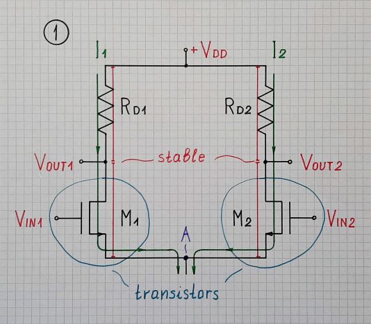
By pairing two identical half pairs, we can assemble the full differential pair. Let's do it in the same order as above by illustrating each of the versions by a separate picture (numbered with 1 - 4) with the corresponding MOSFET implementation from Razavi's book. Now two single-ended input voltages drive the sources; so there are two kind of input signals - common-mode input voltages (when changing them simultaneously with the same rate, in the same direction... and differential-mode input voltages (when changing them in the same manner but in opposite directions).
1. Transistor - resistor pairs. Now everything is doubled - two constant currents flow through constant resistances and create two stable voltage drops across them. We take the difference between the two single-ended output voltages as a differential output. In common mode, both currents stay constant; so, all voltages are stable. At differential mode, the two drain currents are complementary (the common source current is steered between the two transistors).

(Razavi, Fig. 9.30a)
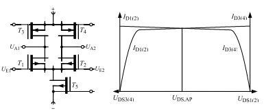
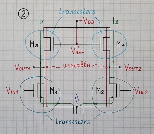
2. Transistor - transistor pairs. In this arrangement, the lower transistors are driving and the upper transistors serve as dynamic loads. In common mode, both single-ended output voltages are unstable; so the differential output voltage is unstable as well and can be easily changed by itself. At differential mode, the two drain currents and output voltages vigorously change.

So, the problem is how to stabilize the unstable single-ended output voltages... or, in other words, how to stabilize the common-mode output voltage (the average value of the two voltages).
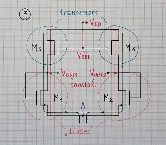
3. 'Diode' - transistor pairs. We remember that diodes can do a good job for us... but they are awkward to implement, have fixed forward voltage... and they are always diodes (see below). Then can we not "reverse" the behavior of transistors - make them work as diodes instead as transistors? Negative feedback will help us do this "magic"; it is enough to connect the gate to drain... and the drain current becomes an input quantity... and the gate-source voltage - an output quantity. First, we can make the lower transistors "active diodes'':

(Razavi, Fig. 9.31a)
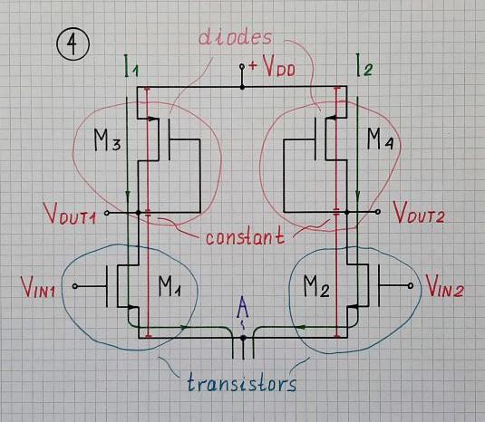
4. Transistor - 'diode' pairs. Then, with the same success, we can make the upper transistors "active diodes":

(Razavi, Fig. 9.46a)
But a problem appears here...
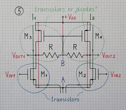
5. Transistor - dual load pairs. We need these "diodes" only when there is no differential mode (i.e., during biasing or at the common mode). At differential mode, we need transistors (dynamic loads) to get a significant gain. So these elements should be able to act, depending on the mode, either as diodes or transistors. Here is the advantage of making diodes through transistors - they can act as both diodes and transistors.
But what determines the behavior of this universal element? This is the presence or absence of negative feedback. When there is a negative feedback, the transistor acts as a diode; when there is no negative feedback, the transistor acts as a transistor. So this will be a feedback acting only with respect to the common-mode output voltage; hence the name common-mode feedback (CMFB). Let's see how the general idea shown in picture 4 is implemented:

(Razavi, Fig. 9.46b)
We are approaching the culmination of our story...
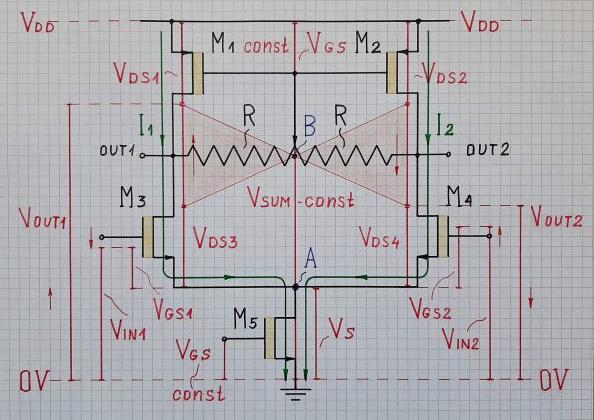
We can obtain the common voltage by a simple summing feedback network consisting of two resistors R in series... and then apply it to both gates of the upper transistors.
Common mode. If, for example, both output voltages try to "move up" (common mode voltage), point B will "move up" as well. The gate-source voltages of M3 and M4 will decrease... their drain currents will decrease... and the output voltages will decrease. As a result, the negative feedback will restore both Vout1 and Vout2. So, at these common-mode voltage variations, M3 and M4 act as "diodes" because of the negative feedback. The voltage drops across them are constant... the common-mode gain is zero.
Differential mode. If we simultaneously vary the input voltages Vin1 and Vin2 but in opposite directions, the emitter voltage of the common point A will stay constant (virtual ground). The common source current is delivered by M1 and M2 and then steered between M3 and M4. The common mode feedback is not active since the average voltage (Vout1 - Vout2) is zero (another virtual ground at the middle point B). So M3 and M4 act as transistors (current "sources"), not as "diodes" (voltage "sources"). They serve as dynamic loads and the differential gain is maximum.
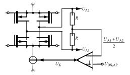
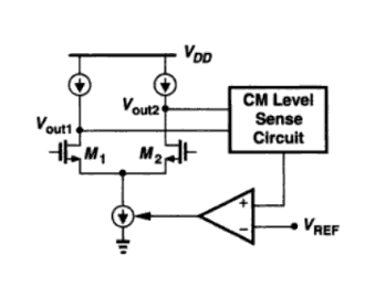
Let's also see how the similar general idea shown in picture 3 is implemented:

(Razavi, Fig. 9.34, page 317)
The op-amp "observes" the common-mode voltage (the average of M1 and M2 drain voltages) and drives the current sink in the source to keep this voltage constant. In differential mode, there is no negative feedback. The source current is steered between M1 and M2; Vout1 and Vout2 vigorously change.
So, CMFB modifies the behavior of both dynamic loads (transistors) in the outputs of the fully differential amplifier at common mode; it makes them act as diodes.
But still, what is the need for the common-mode feedback?
Due to the huge gain, the outputs of the differential amplifier with dynamic loads look like hypersensitive scales that cannot be easily balanced. So the output voltages Vout1 and Vout2 can hardly be held between the supply rails and they easily reach them. This can only be done with the help of the stabilizing negative feedback.
In the differential amplifier with single-ended output, both bias and input voltage affect the same output... and the negative feedback fixes the output voltage to the desired "position" (somewhere between the rails).
In our fully-differential amplifier, these functions are separated - the bias current affects only both single-ended output voltages while the input differential voltage affects only the difference between them. This difference is floating and the bias current should first set it in the middle "position" between the rails... and then keep it there. As it is too hard because of the dynamic loads, there is a need for another negative feedback to do this work... and this is the common-mode negative feedback. It will keep constant the common output voltage (the average of Vout1 and Vout2) regardless of any interferences that attempt to change it.
So "common-mode" here implies "common-output voltage", not "common-input voltage". CMFB exactly means "negative feedback that keeps the common (averaged) output voltage at some desired level between the rails".
Finally, after we revealed the secret of the fully differential amplifying stage with CMFB described in Razavi's book, let's get back to the beginning of the question and have fun with the colorful picture of the complete circuit (it represents, in a more attractive way, Fig. 9.46b from Razavi's book).

