5
\$\begingroup\$

I'm routing traces between a microcontroller and a TFT display (24-bit RGB, clock frequency at 18 MHz).The stackup is:

  • L1 - Signal
  • L2 - GND (solid layer)
  • L3 - PWR (solid 3.3V in the region of interest)
  • L4 - Signal

Components are only on top in order to reduce manufacturing cost (it also explains the choice of a 4-layer stackup).

I designed a first version of this board which worked fine and allowed to develop and test all the software. Now, I'm currently designing a new board version which some mechanical constraints. Some signals were a bit noisy but display worked fine. I would like to improve the routing a bit.

I see two different strategies to route the signals between the MCU and the display. I guess it is understandable that I cannot route only on the top layer even though it would be ideal... The screenshots below are only first drafts and not layout for production.

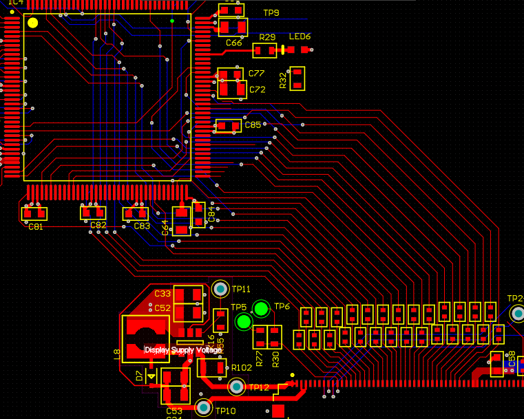
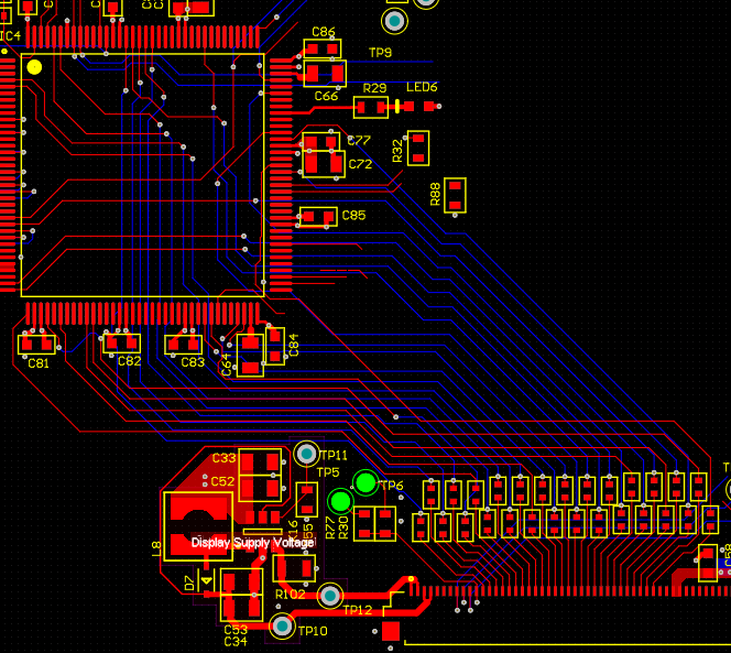
  • Option 1 : that is the option I used in the first boards, vias are both on the MCU side and on the connector side (just before the network of 0 ohm resistors)

Option 1

  • Option 2 : vias are concentrated around the MCU.The goal was to have the return current path goes through the MCU decoupling capacitors to jump from the 3.3V plane to the ground plane.

Option 2

Questions:

  1. Is any of these options better from the point of view of signal integrity/EMC?
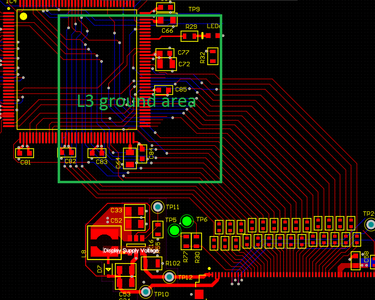
  2. Option 2 makes me want to have a ground area within the power plane (L3) and vias between L2 (ground plane) and L3(ground area within power plane), so the return current path can freely jump from L3 to L2 and the other way around (see picture below) Is it something which would make sense? I've never seen such a design choice in other PCB layouts but I didn't see people routing TFT display on L4 PCB either.
  3. Is there a better way to solve it?

Option 2 with ground in L3


EDIT 1: Even though the question is not about length matching, I give the numbers here to justify why I didn't do any length tuning.

Clock frequency < 18 MHz <=> Period > 55 ns

For a signal speed in PCB is 15 cm/ns and an allowable skew of a quarter of the period, it gives 2 meters. I believe the mismatch of 3 cm in the examples above is not important.

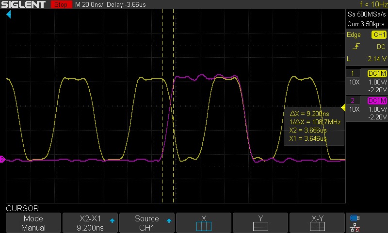
EDIT 2: Quick measurement of a data line (purple) and a clock line (yellow) on the current board with a screen connected and running (it is not a proper 10/90% measurement). I don't really trust these numbers because it is a 100 MHz scope with a 100 MHz probe (20 pF probe). However, it seems to fullfil the 12 ns setup and hold time requested for the screen. Drive strength on the MCU is at the lowest settings (it divides the rising time by two at the highest setting but it introduces some ringing as much as the scope can tell).

scope_rising edge

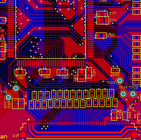
This figure is from the first revision of the board with a layout close to option 1 but with signal lengths 3 cm shorter and a mismatch between lines of 3 cm. Screenshot below.

first revision

EDIT 3: CONCLUSION (EMC testing for CE mark)

Since my last edit, we had the board manufactured. We went for the simplest way possible. We didn't length match the signals, we didn't use controlled impedance PCB, we had a solid ground plane in L2, solid 3.3 V plane in L3. We routed based on option 2 with the vias close to the MCU. Testpoints were added on the bottom of the PCB for each line (for testing with a bed of nails).

The board was functional. We had the chance to go through EMC tests for the CE mark (for home products). The board passed the radiative immunity tests (criterion A since everything was functional) and the radiative emission tests (30 MHz to 400 MHz). Some harmonics from the 25 MHz oscillator (used for the MCU) was actually visible (starting at 425 MHz, 450 MHz, 475 MHz, etc.) and not far from the limits for the CE mark. After some testing, the problem seemed to be gone without the screen connected to the board. We ended up replacing the O ohm resistors on the RGB and clock lines by some ferrite beads. That gave us an extra margin of 5 dBV/m on the worst peak.

Norms used for CE marking:

  • for radiative emission tests: EN 61000-6-3
  • for radiative immunity tests: EN 61000-4-3

I cannot tell that the board was routed the best way possible but it seems to be enough for our requirements. I hope this result will be useful to other people.

\$\endgroup\$
8
  • \$\begingroup\$ You should be length matching the signal traces as well, so it's more complicated than that. \$\endgroup\$
    – Ron Beyer
    Commented Feb 17, 2020 at 4:10
  • \$\begingroup\$ Actually, the clock frequency being <18 MHz, I then believe length matching is not critical. Clock period is > 55 ns. For a skew of half of the period ( 27.5 ns), it would lead to a length of 3.8 meters (15 cm/ns in PCB). \$\endgroup\$
    – Marmoz
    Commented Feb 17, 2020 at 10:13
  • \$\begingroup\$ Layout aside, those SMD components next to the connector look like series resistors. No decoupling caps? Bunch of small ones there would probably make a big difference for EMC, at the expense of space & BoM. \$\endgroup\$
    – Lundin
    Commented Feb 17, 2020 at 11:51
  • \$\begingroup\$ @Lundin Yes, correct, they are 0 ohm 0402 resistors for now. They are supposed to be there just in case... Like here " The emission decrease that results from RGB signal was obtained by adding in series the resistance on each RGB and clock line." (unisystem-displays.com/en/news/emc-test.html). Do you mean using decoupling caps on data/clock/sync lines? Have you some references about this technique? Thank you \$\endgroup\$
    – Marmoz
    Commented Feb 17, 2020 at 12:12
  • \$\begingroup\$ @Marmoz The clock frequency is irrelevant in this case. You need to be aware of the slew rate (rise time) of the signal. This is the restricting speed, and the frequency of concern is 1/rise time. \$\endgroup\$
    – DerStrom8
    Commented Feb 17, 2020 at 12:23

1 Answer 1

3
\$\begingroup\$

Is any of these options better from the point of view of signal integrity/EMC?

Assuming your RGB signals are somewhere between 1.8V and 3.3V logic and given the fact there are single-ended signals, they will be prone to emission. If this is indeed on your concern list, I would recommend a couple of options which I've used in my past experiences:

  • Use either layer 2 or 3 to route your signals, locally switching either the ground or power plane to outer layers : this is probably more work than you've already done, but by burring the traces inside the PCB, you can effectively shield them from outer world if properly implemented. In my view, this is the most effective technique but could be tricky to implement (eg. put a lot of consideration in the ground return).
  • Add RC filter to the output of the MCU (it can be 0-ohm jumper and unloaded capacitors to start with): this filter would allow you to round-off the sharp edges of your signals, dramatically reducing the energy in the harmonics of the signal. However, be careful with this method, you are effectively degrading the signal quality and could end-up with malfunctioning displays. Make sure the signal stays in the recommended RGB electrical specifications. Note that you could use a ferrite bead to replace the resistor element, it sometimes can help to reduce the emission at high-frequency more effectively.

Note that if you have a perfectly shielded enclosure, do NOT put too much thought on these as you may just be fine relying on that faraday cage.

Option 2 makes me want to have a ground area within the power plane (L3) and vias between L2 (ground plane) and L3(ground area within power plane), so the return current path can freely jump from L3 to L2 and the other way around (see picture below) Is it something which would make sense? I've never seen such a design choice in other PCB layouts but I didn't see people routing TFT display on L4 PCB either.

It makes a lot of sense, I would do the same thing and clear off the power plane to let ground flow instead. Be sure to use a bunch of vias to tie them up together and you may want to tie the MCU to that ground plane too.

Is there a better way to solve it?

In terms on functional implementation, I would say you are on point here. Just to be sure, have you sized the trace width so that their impedance is 50-ohm (or whatever the target impedance of RGB signals is)?

I would like to mention that the clock frequency isn't what should worry you for the length matching part. You should consider the rising and falling edges of your signals and check to see if your traces can be considered lumped transmission lines, for that I would recommend Howard Johnson's rule of thumb and use this calculator (or make your own): http://fullychargd.blogspot.com/2017/02/transmission-line-rules-of-thumb.html

In this application, I would estimate the rise time to be 2.5ns and the effective dielectric to be 3.2 (for stripline). A mismatch of 65-70mm or lower would do just fine.

One more thing you may want to consider is to add ESD protections near the display connector, in case you are worried about damaging the MCU during assembly or display swap. I know it's a lot of diodes and it could be overkill if your assembly line is up to standards, however, do weight the pain, money and energy waste into replacing the MCU :)

\$\endgroup\$
14
  • \$\begingroup\$ Thank you for your extensive answer! Yes, signals are 3.3V single-ended. A few questions 1/ Could you explain a bit more how to conclude that the length mismatch should be lower than 65-70mm? I thought this rule of thumb was to consider the track as a transmission line. Below the threshold, it is considered as a ideal capacitor, and a transmission line above. 2/ Do you advise option 2 over option 1? 3/ In this case, there is only a non-shielding enclosure around the board. \$\endgroup\$
    – Marmoz
    Commented Feb 17, 2020 at 14:56
  • \$\begingroup\$ 1/ Ha sorry, it wasn't really clear. I am looking into propagation delay, which is how far the signal has traveled, to "quantify" the phase mismatch between the RGB signals. If the trace can be considered a lumped circuit, not so much to worry about signal integrity and, therefore length matching. For a distributed circuit, any side-effects (like reflexion, ringing, etc.) will come into play 2/ I would prefer option 2 bis, with the L3 ground plane. 3/ Ouch, I would recommend visiting the first few options I mentioned. One more thing, do you have access to drive-strength control on your MCU? \$\endgroup\$
    – eeintech
    Commented Feb 17, 2020 at 15:29
  • \$\begingroup\$ 1/ Line impedance should not also matter if the total length is below the critical length, no? The drive-strength control is already set to the minimum setting on the MCU (and the display works fine). \$\endgroup\$
    – Marmoz
    Commented Feb 17, 2020 at 16:29
  • \$\begingroup\$ Yes, line impedance wouldn't be critical in your case, but it's always good practice to have it set right and get used to set it correctly for each new design. Given you can control drive-strength, you may not need the RC filter I mentioned. Have you looked into the shape of the signal? Is it meeting the RGB requirements? Do you have enough margin (eg. it could work for this combination of board and display but might not with a different setup)? \$\endgroup\$
    – eeintech
    Commented Feb 17, 2020 at 16:35
  • \$\begingroup\$ OK! I just added in the original post a measurement of the signals. It does meet the requirements (frequency, setup and hold time...). I don't know how much to trust them since the scope is probably very limiting. However, the extra capacitance of the scope does not seem to make the signals go outside the requirements... \$\endgroup\$
    – Marmoz
    Commented Feb 17, 2020 at 16:55

Your Answer

By clicking “Post Your Answer”, you agree to our terms of service and acknowledge you have read our privacy policy.

Not the answer you're looking for? Browse other questions tagged or ask your own question.