0
\$\begingroup\$

I am trying to simulate an inverter with 4 ideal switching devices in LTSpice. I have the compensator working, however I don't the correct equation in terms of calculating the duty cycle.

What I have tried is this:

V=limit(abs((V(V_OUT))/391 + 1.1*V(Icomp)/391) ,0.01,0.99)

Which is essentially limiting the duty cycle from 0.01 to 0.99 and adds sinusoidal voltage output scaled down by 391 and the compensator signal. Is there a problem in the way I generate the duty cycle signal, because it has distortion and reduction in amplitude of the output signal when inductive load is simulated.

NOTE: ADC range is from 0-686, 391 is just a fixed scaler.

I could provide more details, but I just want to find out the correct way of calculating the duty cycle. Nonetheless if more information is needed I will post it.

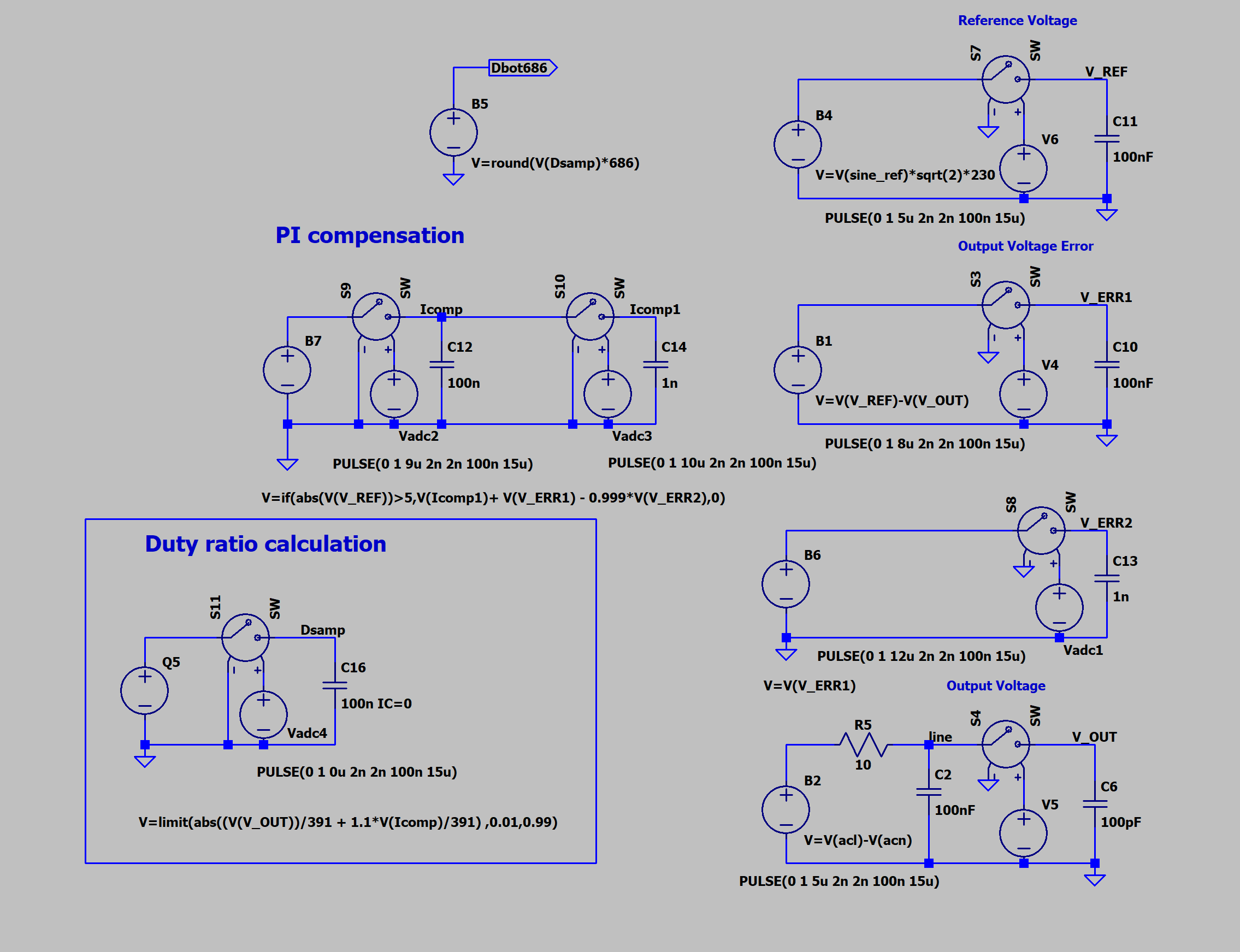
Simulation for PI controller is as follows: enter image description here

\$\endgroup\$
2
  • \$\begingroup\$ Anyone, please? \$\endgroup\$
    – Rr Bb
    Commented Feb 21, 2020 at 14:01
  • \$\begingroup\$ When you say inverter, do you mean a power transistor (H) bridge, or a CMOS inverter? I see nothing related to the latter, but it's hard to read what you have done. I tried replicating it, but there are missing nodes. I tried supplementing them what I thought would fit, but I see a sampled sine at the output, not what you'd expect from an H-bridge. I also see a PI compensation, but nothing that resembles it? Maybe an error amplifier (B7) with s&h afterwards? Could you post a link, or a picture, of what you're trying to make? \$\endgroup\$ Commented Feb 21, 2020 at 18:56

0

Your Answer

By clicking “Post Your Answer”, you agree to our terms of service and acknowledge you have read our privacy policy.