17
\$\begingroup\$

In the following NOT transistor circuit diagram, the current flows through the 1K resistor and through the LED when the switch is open. This turns the LED on. When the switch is closed, however, the transistor turns on and the current flows through the same resistor, but bypasses the LED, turning it off.

Why isn't the current split between the transistor and the LED? Why does the transistor path get all of the current when the switch is on? Shouldn't there be some current flowing through the LED as well? Why is it being starved of all the current? What would happen if we moved the 1K and placed it in series with the LED? Would it cause a short circuit? Let's say you replaced the transistor, the switch and the gate resistor with a small resistor. Would it split the current then?

I prefer a math-free explanation using analogies since my working memory isn't optimized for it. In other words, my brain has a slow ALU and a tiny set of small registers.

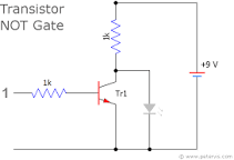
enter image description here

\$\endgroup\$
12
  • 7
    \$\begingroup\$ LEDs (diodes in general) can only pass significant amounts of current if there is enough voltage across them. Like a pressure valve. The BJT forces the voltage acrpss the LED to be too low \$\endgroup\$
    – DKNguyen
    Commented Feb 26, 2020 at 15:40
  • \$\begingroup\$ I understand the switch is in terminal "1" connecting to another source? Can you please clarify? \$\endgroup\$ Commented Feb 26, 2020 at 15:41
  • 4
    \$\begingroup\$ Current does split between the transistor and the LED, but since most visible light LEDs need a few volts before much light comes out, the tiny bit going through the LED produces no meaningful light. If you had a long wavelength IR LED that operated at a lower voltage, this circuit wouldn't work so well. \$\endgroup\$ Commented Feb 26, 2020 at 15:41
  • \$\begingroup\$ OK. So the transistor is stealing all the current? or most of it? \$\endgroup\$
    – user148298
    Commented Feb 26, 2020 at 15:42
  • \$\begingroup\$ One explanation claimed that there is no potential difference between the LED and ground when the transistor is turned on. If it's the case, then no current should be flowing through the led at all? Correct? \$\endgroup\$
    – user148298
    Commented Feb 26, 2020 at 15:44

8 Answers 8

27
\$\begingroup\$

tl; dr version: The transistor's Vce(on) is lower than the LED's Vf, so when the transistor is on the LED is well below its Vf threshold and so doesn't conduct.

LEDs, Vf and Hue

The LED, like all diodes, has a forward anode-to-cathode voltage, Vf. The LED will not conduct until the Vf threshold is reached, after which current climbs rapidly.

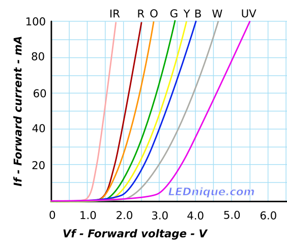
This Vf voltage varies depending on LED type, between 1.1V for an infrared type up to 3V or so for a blue or white LED. These different Vf thresholds come from the materials used to make LEDs in different colors. In comparison, ordinary silicon diodes have a Vf of 0.7V.

Here's a pretty graph showing the different Vf behaviors for a variety of LED types.

LED Vf Characteristics

From here: http://lednique.com/current-voltage-relationships/iv-curves/

Bipolar Junction, What's Your Function

The bipolar transistor on the other hand will have a minimum collector-emitter voltage, Vce, when it is turned on - that is, Vce(on). This Vce(on) voltage is about 0.2V. The reason why is beyond the scope of this discussion. Just know that it is, otherwise we go down the Ebers-Moll rabbit hole.

Bipolar Is Dragging Me Down

So in this circuit, when the transistor is on, it drags down the LED anode-to-cathode voltage to the transistor's Vce(on) of 0.2V, well below the LED Vf of 1.1V or higher. You'll see this on the Vf graph above: 0.2V is well into the no-current zone of all the LED types.

As a result, when the transistor is on, there is (almost) no current flow through the LED. The LED Vf threshold isn't met, so it doesn't conduct. Electrons don’t find their way to holes, no quanta of energy get emitted as photons, and the LED stays dark.

\$\endgroup\$
3
  • 1
    \$\begingroup\$ That diagram is inaccurate. First, different LEDs of the same color can have different characteristic curves; a graph like this presents only generalities. Second, the overall trend should be toward higher voltage for shorter wavelengths, since shorter-wavelength photons contain more energy; the green and yellow curves, for example, appear reversed. Third, a "white LED" is generally a blue LED embedded in a yellow phosphor, and so it will have the same characteristic curve as a plain blue LED. \$\endgroup\$
    – jeffB
    Commented Feb 27, 2020 at 17:16
  • 5
    \$\begingroup\$ Go hassle the page author. I’m only illustrating a general idea of Vf. \$\endgroup\$ Commented Feb 27, 2020 at 17:41
  • 2
    \$\begingroup\$ Can't hassle the page author if there's no contact info, only "share" buttons. Your answer here is good (worth my upvote), and the diagram specifics aren't important to it, but I get twitchy when I see a "pretty" diagram that's got clear factual errors. I get twitchier when I see the diagram propagating. \$\endgroup\$
    – jeffB
    Commented Feb 27, 2020 at 20:36
20
\$\begingroup\$

The mathematical truth is that the current will actually split between the LED and the transistor, but the current that flows through the LED will be effectively zero.

The LED only starts to draw significant current when the voltage across it gets relatively close to the normal operating Vf (typically around 2-3V for visible light LEDs). The transistor when saturated as in this example, will have maybe 100mV across it, so probably less than a nA of current will flow.

The LED does not behave like a resistor, it's nonlinear.

If you move the transistor collector to the +9V node, the LED will remain on (assuming a good 9V supply) but the transistor will get very hot and will quickly be destroyed.

A more useful idea might be to add a resistor in series with the transistor collector. If the resistor is high enough value, the LED light will just dim and will not go out entirely when the transistor turns on.


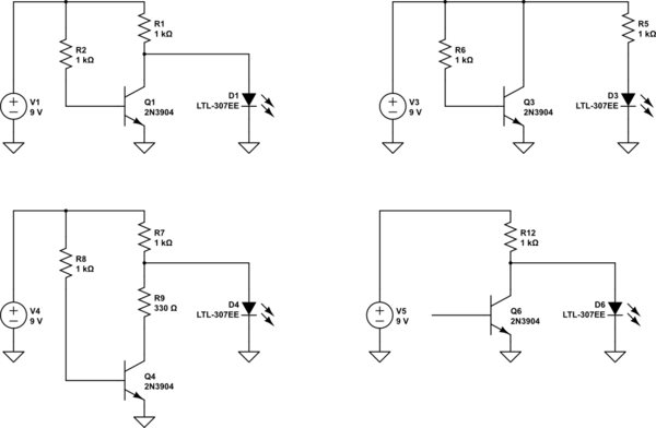
Edit: Here is a simulation of the various scenarios:

schematic

simulate this circuit – Schematic created using CircuitLab

enter image description here

D1 conducts only 3nA according to the simulation. D3 conducts the same as D6 (but the transistor Q3 is not long for this world). D4 conducts only 2.4mA so it dims a bit but remains illuminated.

\$\endgroup\$
4
  • \$\begingroup\$ If you measured the voltage drop between the emitter and collector when the transistor is on, it would be zero? Correct? If so, then there should be no current through the LED? \$\endgroup\$
    – user148298
    Commented Feb 26, 2020 at 15:51
  • 2
    \$\begingroup\$ Yes, exactly, that's the ideal situation. In reality the transistor will have a bit of voltage drop, but not nearly enough to illuminate the LED. \$\endgroup\$ Commented Feb 26, 2020 at 15:52
  • \$\begingroup\$ One last one. I can't picture your circuit with the transistor collector moved to the +9V node. \$\endgroup\$
    – user148298
    Commented Feb 26, 2020 at 15:57
  • \$\begingroup\$ @user Emitter follower. Google it. Won't act as a switch. \$\endgroup\$
    – DKNguyen
    Commented Feb 26, 2020 at 15:59
5
\$\begingroup\$

Roughly speaking, when the transistor is on, you can replace it with a piece of wire... and the LED will be totally shunted. So, all the current will flow (be diverted, steered) through the "wire". You can remove the LED and all the elements except the 1 k collector resistor and the power supply. Your circuit will consist only of two elements - the resistor and power supply... and will do nothing.

When the transistor is off, then you can remove it (together with the 1 k base resistor, input switch and input voltage source). Now your circuit will consist of three elements - the resistor, power supply and LED that will shine.

In the common case (non-ideal transistor), think of the parallel-connected collector-emitter part and LED as of a current divider... only consisting of two non-linear resistances.

Another (I think better) viewpoint at this connection, is to think of the collector resistor (R1) and transistor (R2) as of a variable "voltage divider" R1-R2 supplying the LED. Then, when "R2" is too low (the transistor is saturated), the voltage produced by the "voltage divider" will be unsufficient to forward bias (light) the LED... as all comments here explain it.

You can use both "current divider" and "voltage divider" viewpoints to imagine the operation of the common-emitter stage. The former is more suitable when the load is low-resistive (your case); the latter - when the load is high-resistive (even open circuit).

\$\endgroup\$
1
\$\begingroup\$

There's yet another way of looking at it, that involves looking at the characteristic curves of the parts involved. Perhaps that helps you figuring out what is going on.

First, figure out how much base current there will be through the transistor when it is on. The base-emitter junction has the characteristic curve of a diode, so you should be able to figure out the current by drawing a load line through the characteristic curve of the base-emitter diode (the load line is a straight line with the slope determined by the 1k base resistor).

Then, using this base current value, select the right Ic vs. Uce curve of the transistor. You can again draw a loadline through this curve corresponding to the 1k collector resistor. In this manner you can find the right Uce value, which is the voltage between collector and emitter.

Using this voltage, look up the current through the LED for this voltage, using the characteristic curve for the LED. (This isn't entirely accurate, because the current through the LED affects the voltage across the collector resistor, but it gives you a close approximation).

For the characteristic curves, you need to consult the data sheets of the parts. If you want to know the solution in principle, choose some exemplary parts for which you can find data sheets with the curves.

You will find that the current through the LED is very small. Much too small for an appreciable amount of light being emitted.

\$\endgroup\$
1
\$\begingroup\$

I'll have a go at the layman's answer. Your circuit can be considered as have only two conditions, When the transistor is ON and the other when it is OFF. In the ON case, the transistor resistance drops very low, and can be considered a straight piece of copper wire between the ground and diode/resistor junction (or if you want to get mathematical, then a resistor of c1ohm). So the supply voltage on the diode is very low indeed (like less than 0.1volts), and well below the diode forward voltage required of it to light up. Diodes of any form require a forward voltage of typically 0.4c to 1.2 volts to start conducting. This voltage threshold is defined by the transistors designed type and effects colour of the photons/light it emitts.

In the Off case, the transistor can be considered a high value resistor, and you could on paper simply rub this component out and review on the basis of what is left in the circuit. In this case the circuit simples to a simple diode in series with a 1k resistor connected to the supply. The diode sees the full supply voltage, and lights up. The 1k resistor is the only compenent limiting the current through the diode, and so needs to be sized to ensure the diodes maximum forward current is not breached. 1k on 10v give 10mA, which is about right for most typical LEDs.

\$\endgroup\$
1
\$\begingroup\$

As to DNKguyens reply it was answered in a couple of ways first off when the transistor sinks the voltage there is none left to flow through the led theoretically playing the Devils advocate we know that there is likely .7 volts left which is far too low (especially) with the resistor is series with the led to make it gate and fire or turn on. So in short the transistor in his diagram shorts all the available power to ground return that normally fires, or gates the led to turn it on or make it emit light. Now one other thing at least some if not all LEDs below light emission voltage levels act like a 1n914 type diode in most instances. I have used this to my advantage in Circuits that I have designed in the past also they can be used as detector diodes in RF circuits but being silicon they only preform at a level of a 1n914 no where near the sensitivity of germanium like a 1n34a.

\$\endgroup\$
3
  • \$\begingroup\$ This is a good answer except for some strange terminology. We use the term "gate" to describe the control pin on a three-or-more-terminal device. LEDs don't have gates. "Fire" in this context would also relate to three terminal devices. I suggest, "0.7 V is too low to cause the LED to conduct and light up". It might be a translation issue but you have no location information in your user profile. Welcome to EE.SE. \$\endgroup\$
    – Transistor
    Commented Feb 27, 2020 at 17:29
  • \$\begingroup\$ He literally signed the answer with location information ;) WB4IVG is a US ham callsign. \$\endgroup\$
    – MrGerber
    Commented Feb 27, 2020 at 18:39
  • \$\begingroup\$ Yep US. Sorry I was not suggesting that. 7 vdc would light an LED that is the accepted drop across most silicon diode devices. As far as Gate or Fire those terms are loosely used in the industrial and commission fields. I had no intent to confuse anyone I was just using terms we toss around while working through problems on projects. \$\endgroup\$ Commented Mar 2, 2020 at 2:28
0
\$\begingroup\$

The gate or the switch is the deciding factor for current to flow in either directions. When the switch in open the base gets no signal and so the transistor is off and all the current has to flow thru the LED bypassing the transistor. But when the switch is closed the base gets a biasing voltage and starts to conduct so much that all the current flows thru the transistor and gets grounded to the negative of the battery so the collector voltage is roughly the voltage across collector and emitter which is not sufficient to make the LED glow even though it is still connected.There is one way to make it glow even when the switch or gate is closed and the transistor is conducting it is by making use of voltage divider.If another resistor sufficiently high is placed between the collector and the point from where the tapping for LED has been taken then when the transistor conducts the voltage gets divided between two segments one is across the 1k resistor and another is across the newly placed higher value resistor which becomes the triggering source even when the transistor is conducting.

\$\endgroup\$
1
0
\$\begingroup\$

The answer here begs another question. First off is this just a mental exercise or are you trying to do. Work? If what you are doing is to turn the led off an on this is a bad way to do it, because it uses current all the time and generates waste heat. Now if you are supplied with unlimited supply power this might not be an issue, although if your supply is a battery this is a whole different story, but it is still bad Engineering practice to use the circuit that you depict. It would be so much simpler to put the led and current limiting resistor in the return leg of the switching transistor then the control voltage simply turns on the transistor or not so the led is off or not. You would only have to make sure that the switching transistor will carry enough current to power the led. The control or Base resistance will depend upon what power that you have available for switching. The power input resistor depends upon how much the supply voltage has to be dropped to be in the correct working voltage of the transistor and the led. And of course whether you use a N or a P Channel switching transistor depends upon your supply voltage being Positive or Negative. This also determines which way you face your diode (led). Your switching voltages polarity must be sourced to your supply or it will have to be run through an inverter of some sort be it another simple transistor switch or inverter ic.

\$\endgroup\$

Not the answer you're looking for? Browse other questions tagged or ask your own question.