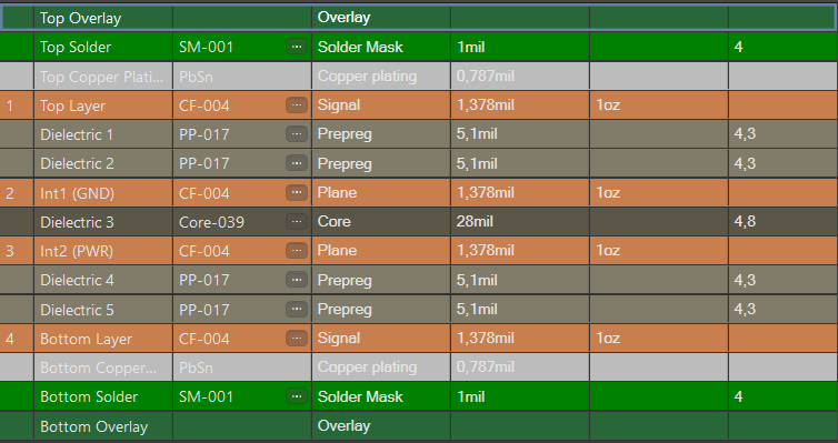
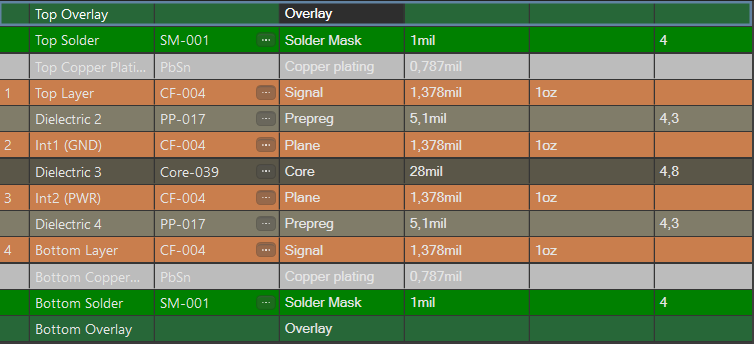
I'm desinging a very simple 4 layer board with a USB connection. I defined an impedance of 90 Ohms (differential) in the layer stackup. This gave me a track width of 0.3 mm with a gap of 0.334 mm, which roughly agrees with my hand calculation. I used the differential pair routing option, matching the suggested measures as close as possible. I do need one pair of vias to get from a SMD connector to layer 3 where the routing is done, but apart from that the trace is a straight line.
However, the signal integrity calculates an impedance of 239 Ohms. This impedance doesn't change, no matter what I do. For test purposes, I changed the trace width, the dimension of the board, the thickness of the substrate and added a via fence around the differential pair traces. None of these measures caused any change to the impedance in Signal Integrity.
Am I doing something wrong? I mean I wouldn't expect the Signal Integrity impedance to be exactly the same, but this is off by a factor of more than 2.5... Has anyone experienced this problem before and found a solution to it? Any help would be highly appreciated.
Edit: I'm using Altium 19.1.8.


