Im using Lattice ECP3 FPGA, didnt found any information about it on the internet.
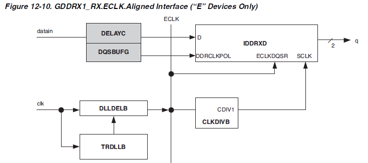
I have ADC which providing me 12bits data on both clock edges, so I used Lattice High Speed I/O Interface:

This Interface latching the ADC data on 24bit bus which compound of the positive edge data (lower bits- 11:0) and negative edge of the data (higher bits- 23:12). my next step is to transfer all this ADC data to FFT block, problem is the FFT need to work on the 12bits data coming from the ADC and not the 24bits, so I need to seperate the data to 2 and send on every rising edge of clock another half of the data, and its important not to lose any sample.
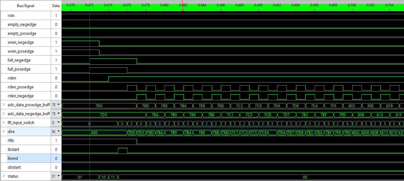
So I already have a working design, I did 2 FIFOs one for the positive edge data and second for the negative edge data, created mux which change its state evey rising edge clock, and when I want to read the data from the FIFOs to the FFT block, I taking one sample from the 1st FIFO and 2nd sample from the 2nd FIFO and so on... I have working synthesis and debuggin:
as you can see the input to the FFT block (dire) gets the adc_data_posedge/negedge_buff as described. but I have strong feeling that this way of implementation is not the right way to make this design. I read that using 2 FIFOs for the same input block could make sync problems and so on..
It could be better if I could take the ADC data bus of 24bits and write to 2 cells of the FIFO at a time in the rising edge of the clock. This way ill create 12bit width FIFO and write to 2 cells at a time and dont need to use 2 FIFOs. there is a possible way to do it?
another way to ask my question is, lets assume you have to design architecture which takes DDR ADC data and store it in the FIFO and then use the FIFO output as input to FFT block. how would you do it?


