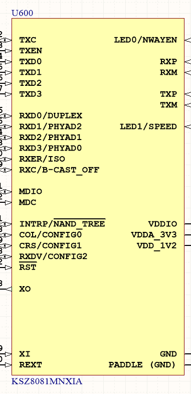
as you can see options strapping pins are multiplexed with RXD# pins .. which are MII interface pins.
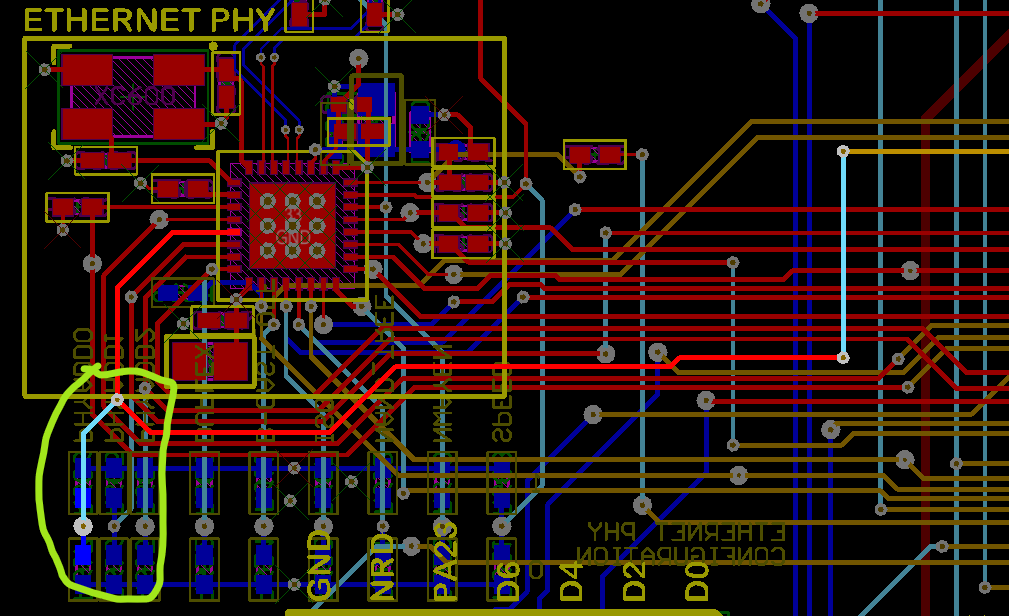
this will make the PCB have "stubs" (connected to MAC + pullup resistors) which is not good in signal integrity wise..
why they didn't build the strapping option on other "non data" pins like LED for example or MDIO .. as much as i know these are just latched at startup of the chip ..
the routing is not mine. its "microchip evaluation board" SAM4E-X-Plained board
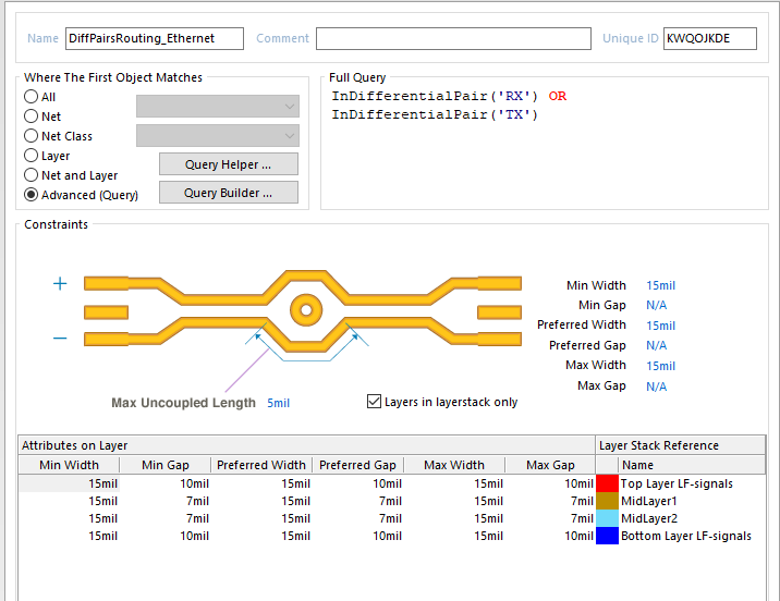
i cant see any rule related to MII only differential ethernet it self which is routed on top and bottom only (layer 6) :
 layer5 is actually power plane (not gnd) i dont know if impedance matching related to it is counted or it must be GND (return path is GND!)..
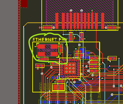
things originally worried about: (note i didnt put them in the question originally because i thought it will be wide and open) - stubs - layer changing - length matching - impedance matching on non-GND layers - signals crossing overeach other - some are (routed opposite of each other for small length) - clock being near edge of board (how close is near?)


