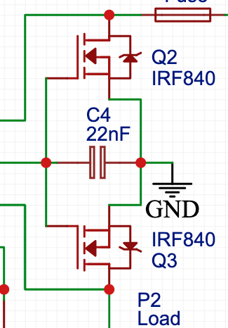
I have a comprehension question regarding the design of a reverse phase dimmer. I have a picture attached of the part of the circuit I do not understand:
The line is connected to the Drain of Q2 and the load is connected to the Drain of Q3. The sources are connected together and the gates are driven by an IC or MCU. So I understand that the complete sine wave can pass the series transistors. Now what I do not understand is why the GND rail is connected to the source of the AC path between the sources of the MOSFETs. Would that not induce high voltages on the GND rail and destroy the low voltage components like the IC or MCU? Or am I getting this completely wrong... Thank you very much for any kind of answer!

