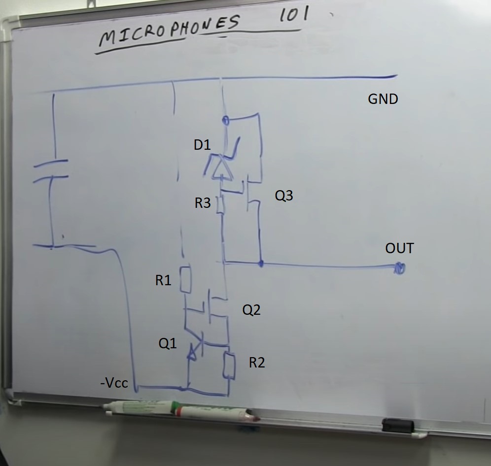
About the following circuit:
*source: https://youtu.be/niZizzHBanA?t=1779
It is described as a negative power supply, where R1, R2, Q1 and Q2 form a current sink and Q3 "amplifies" the zener voltage, keeping a stable voltage between its drain (GND) and source (out).
So I have a few questions. I'll start just with the current sink. I've reduced it and isolated it as below:
1) Can I call the current sink configuration a series feedback pair?
I know it has the benefits of the high output impedance of the JFET, and the high gain of the BJT which allows a proper negative feedback. So the way I see it works like this. In initial conditions, Q2 gate is assumed at 0V, since there is still no current flowing through Q1. So Q2 will allow a \$I_{DSS}\$.
At the next moment, R2 will have a \$V_{BE}\$ across it from Q1 as long as \$I_{Q2}*R2>0.7V\$. That should be enough to keep Q1 saturated and R1 will set Q1 collector current. The voltage drop at R1 will set the voltage at Q2 gate.
2) Should Q1 be really saturated? I can't see other way, since there is really no restriction for its base current.
It is also clear how negative feedback works. If \$I_D\$ in Q2 tends to increase, \$V_{BE}\$ in Q1 tends to increase, also increasing Q1 collector current, that makes \$V_{GS}\$ more negative and regulates the disturbance.
R3 is the load and operating current in the example is \$\frac{V_{BE}}{R2}\$ , calculated for a 2.5mA renders \$R = 269\Omega\$.
J2 at left of the circuit is there just to check the actual \$I_{DSS}\$ for this part in LTspice, and that is equal to 5.19mA.
Simulations showed excellent results, ranging from R3 short circuited (green) up to 4.48k (pink). Last step was to 5.6k (not displayed below), that started to reach the compliance voltage.
3) How is it possible that \$V_{GS,Q2}\$ goes down to -14.5V and there is still current flowing through its drain and source?
According to this part datasheet: LSK489A, its pinch off voltage should be about -1.7V for a \$V_{DS}\$ of 10V at 25C. In my example, \$V_{DS}\$ ranges from -470mV for the 5.6k load to -14.3V for the short circuit. But any \$V_{GS}\$ more negative than ~ -1.7V should not allow the calculated current of 2.5mA in R2.
How is this possible and suggestions for fixing it, if needed. Changing R1? That still seems weird to me, because \$V_{GS}\$ and \$I_{DS}\$ are related by the
JFET basic equation: \$ I_{DSS}(1-\frac{V_{GS}}{V_p})^2 \$
Where \$V_p\$ is the pinch-off voltage.
So how is \$V_{DS}\$ of Q2 supposed to accomodate variations in voltage in order to keep the \$I_{DS}\$ when its \$V_{GS}\$ is being held by the voltage drop in R1?
I will elaborate further questions on the actual "zener amplified regulator".
EDIT1: fixed equations.


