3
\$\begingroup\$

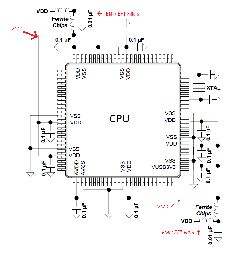
In microchip AN2587: EMI, EMC, EFT, and ESD Circuit Design Consideration for 32-bit Microcontrollers Page 50 . The following power connection for Vdd is recommended (similar diagram in datasheet) Vdd.

I drew on the picture 2 marks called vcc-1 and vcc-2 , which will become net labels in the pcb desgin.The Board is a 4-Layer stackup (Signal-GND plane-Power plane-Signal) .Now I am lost in what will the power plane be connected to ?

1- power plane is Vdd or cut into 2 parts 1 is vcc-1 and other is vcc-2 ?

2- if Power plane is Vdd, how should Vcc-1 and Vcc-2 be routed? top or in the power plane ?

3-Option #3 : use different 4-layer stack up (Signal+power- GND plane -GND plane-Signal+power) No vdd plane (idea taken from Henry ott EMC book )

\$\endgroup\$
2
  • \$\begingroup\$ "to enhance an application's immunity in electrically noisy environments and survivability of EMI, EMC, EFT, and ESD events" LOL, you must absolutely avoid EMC events! They're the worst \$\endgroup\$
    – Huisman
    Commented Apr 12, 2020 at 6:14
  • \$\begingroup\$ My power plane is vcc. I don't know why there's a vcc1 and vcc2. Unless you're separating avdd. But it doesn't look like you are? \$\endgroup\$ Commented Apr 23, 2020 at 12:21

3 Answers 3

4
+50
\$\begingroup\$

It seems people have different opinions about the subject of grounding, however the way I would do it is by using traces instead of the Power planes on bottom layer, and remove the local ground plane and instead vias directly to the middle GND plane as shown in the schematic of the microchip app note. Also i base on what i read in the same book you mentioned (EMC compatibility). have you read all chapters ?

Chapter 17 page 686 :

Qoute:"

  1. Partition mixed-signal PCBs with separate analog and digital sections.

  2. Do not split the ground plane; use one solid ground plane under both analog and digital sections of the board."

Which means one ground plane under the signal layer which has its physical area partitioned (imaginary separation) between Sections ( Analog alone , High speed digital alone , I/Os alone ) . The component placement and routing should be not interfere with other sections.

Chapter 11 page 461:

Qoute:"

  1. At high frequencies, the most important criteria is to reduce the inductance in series with the decoupling capacitors.

    2.The number one rule of decoupling is to have the current flow through the smallest loop possible."

According to the above:It doesnot look like the approach you are using provides the shortest path for current to the main ground plane.

EDIT: There is also a discussion in chapter 3 section 3.2 that discuss Signal grounding and mentions 3 types:

  1. Single-point grounds ( like what you are doing )
  2. Multi-point grounds (like what most people propose)
  3. Hybrid grounds ( a mix between the 2 above as name suggests)

To summarize what the author says:

Single-point is most effectively used at low frequency up to 1Mhz max. It controls how to direct the ground current to flow where we want it. This can be used to decrease noise in sensitive analog circuits. While Multi-point ground systems minimize the ground noise voltage by minimizing the ground impedance which is more important at high frequency digital circuits.

The confusion might be from considering the common impedance coupling shown in figure below EMC compatibility Figure 3-20
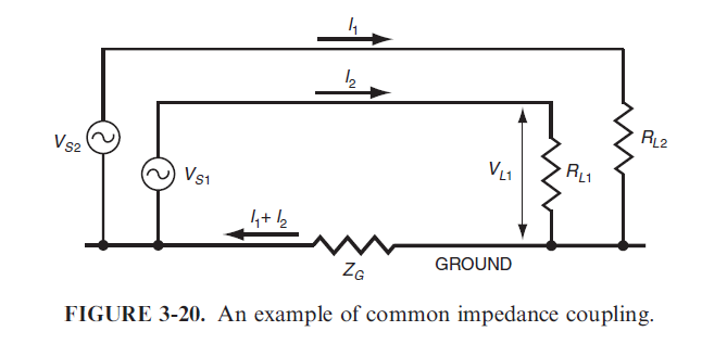
In this circuit VL1 = VS1 + ZG * (I1 + I2).

This means that the voltage across the load RL1 is no longer a function of I1 but also a function of I2.

Remember: A high-impedance ground at high frequency is caused by too much inductance while at low-frequency this is caused by too much resistance.

Single-point grounds overcome this by separating ground currents that are likely to interfere with each other and by forcing them to flow on different conductors. This approach is effective at low frequency. However, the signal current paths and long lead lengths associated with single-point increase inductance, which is bad at high frequencies.
\$\endgroup\$
1
  • \$\begingroup\$ Thank you for the well written answer . I actually have read parts of the book by Henry Ott , I will be reading it all , as it seems there is much that i have missed. \$\endgroup\$
    – ElectronS
    Commented Apr 21, 2020 at 17:43
2
\$\begingroup\$

Sadly No one answered so after Some thinking and reading mainly the Answer of Olin in Decoupling caps, PCB layout . Also this question was Helpful PCB microcontroller layout in a mixed-signal system

I believe I have come up with a solution.

The Stack up will be:

1- Top: Signal + local GND for micro only

2- GROUND PLANE continuous

3- VCC 3.3v PLANE continuous

4- Signal + 2x local Power islands for micro only

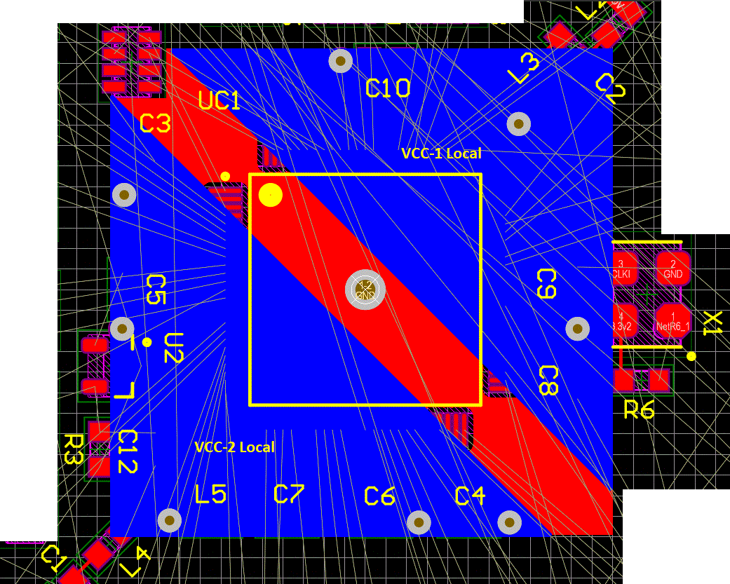
Note1: The local ground for micro-controller will be connected to the GND plane using a BIG via in the middle.

Note2: The local power is 2 pieces Vcc-1 and Vcc-2 each has a connection to Power Plane after the L-C-L network.

Your Comments are very welcome

My layout is now like this :

In first image top layer is shown , purple is solder mask (shown here to make capacitor pads clearer ) . The line under C9 is the 24mhz clock . all caps are 100nF 0603.

Second image shows the bottom layer . the 2 triangles are Vcc-1 and Vcc-2 . they are connected to main Vdd plane on the top layer after L-C-L network.

Middle layer are not shown in both images to avoid over crowding the view.

enter image description here

enter image description here

\$\endgroup\$
3
  • \$\begingroup\$ Single big via? How much DC current would you estimate passes that via? What frequency AC signals (such as SPI clock) you have on the MCU that need ground currents to pass through that single via? \$\endgroup\$
    – Justme
    Commented Apr 16, 2020 at 20:15
  • \$\begingroup\$ it is just a via , just made it a little bigger (hole=1mm , diameter 1.6mm) to reduce inductance \$\endgroup\$
    – ElectronS
    Commented Apr 17, 2020 at 0:56
  • \$\begingroup\$ The circuit looks fine , however the Power planes on bottom layer seem pointless , you can use thick traces and that would be enough i guess \$\endgroup\$
    – Sarah
    Commented Apr 21, 2020 at 16:41
1
\$\begingroup\$

I would never design a power distribution circuit like what's shown in the OP's post.

Here's what I would do:

  • Layer 1, no signals; no power

  • Layer 2, GND (Vss on the schematic)

  • Layer 3, Vdd

  • Layer 4, signal (X-routing)

  • Layer 5, signal (Y routing)

  • Layer 6, GND (Vss)

Keep going for as many layers as is needed to route your board.

You could consider moving the Vdd plane under the 2 signal layers, though this would make the via length longer and so increase its inductance.

Then via down to the Vss and Vdd planes for making the connections to the chip. Place the SMD decoupling caps as close to the chip as possible, and connect them to the Vss and Vdd planes with vias.

Never connect decoupling caps for a high-speed device to the device with traces if planes are available.

If you think you need ferrite beads or something similar in the Vdd net, put them where the power comes into the plane. But I would do a PDS analysis/modeling to see what effect, good or bad, they may have. Just sprinkling ferrite beads onto the Vdd nets could cause more problems as now you're setting up more resonances that could be excited by switching transients in the CPU.

\$\endgroup\$
4
  • \$\begingroup\$ So what you mean is you donot like the idea of the T-Filter consisting of ferrite and capacitors that is shown in microchip appnote ?? \$\endgroup\$
    – ElectronS
    Commented Apr 21, 2020 at 18:12
  • \$\begingroup\$ And regarding the GND island under micro-controller to connect to gnd plane shown in my answer to the question , that also is bad ? \$\endgroup\$
    – ElectronS
    Commented Apr 21, 2020 at 18:13
  • \$\begingroup\$ Also you didnot say why use 6 layer stack up instead of the 4-layer stack up in question ?? \$\endgroup\$
    – ElectronS
    Commented Apr 21, 2020 at 18:14
  • 1
    \$\begingroup\$ No I don't like T-filters in power nets destined for high speed devices. The less inductance in the PDS, the better. The GND island may be OK. I would need to see the entire PCB. I would prefer a full GND plane (Vss) over the entire board. 6 layer vs 4 - I said keep going for as many layers as needed. Current design I'm associated with has 30 layers. I usually don't start paying attention to layer count until we get over 24. \$\endgroup\$
    – SteveSh
    Commented Apr 21, 2020 at 19:11

Your Answer

By clicking “Post Your Answer”, you agree to our terms of service and acknowledge you have read our privacy policy.

Not the answer you're looking for? Browse other questions tagged or ask your own question.