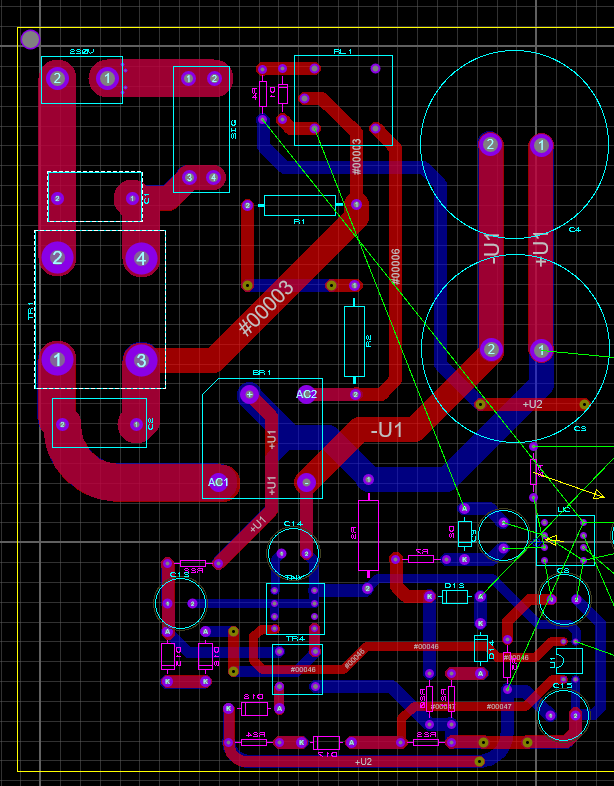
[~15A.] The question is, how do I make the current pass from the top to the bottom if the component pads are small or very small?
This might be an XY problem. Are you asking if 15A can go through a component lead to get to the other side? I do not see any surface-mount (pad) components. Yes, provided the hole/lead diameter is large enough, a through-hole can handle 15A. But I don't think this is warranted; I'll explain below.
Can I put vias near the pad, and how?
Yes if you want. In KiCAD, mouse over the track, X to begin drawing a wire, click on track, and press V for via. Note the top and bottom track must have the same net (name) else it will fail.
Is it necessary to add vias next to each component?
Usually not, except for high currents on thin tracks. 300mil is a pretty wide track, good for about 10A on a standard FR4 board. Two 300mil tracks (top and bottom) should be good for 17A, so is a good choice for 15A.
The frequency is about 2 MHz. Is parasitic [capacitance] formed between the same routes if they are on the top and bottom, or is it ok?
If the tracks are electrically the same then no, parallel tracks on top/bottom do not add significantly* to the capacitance. They would however, if one side was a different net, at a different voltage. That's what a capacitor is - two plates with a dielectric between them. Short a capacitor's leads: is it still a capacitor? No.
*They do very slightly, due to the increased surface area, but this is very small so is irrelevant for this part of the circuit.
Is the voltage the same on the Top and Bottom on the same route? What rules should I take into account in this case?
It is very hard to see where the "both-side-routed" tracks are in the schematic because the tracks are opaque. There might be some setting for this, but I know that pressing the F9 key to display in "legacy" mode (and F11 or F12 to revert) will enable/disable transparency. Try that and see if it helps.
If the tracks are the same net, and connect to the same component leads, then their voltages will be the same. If one were narrower than the other, then the narrow one will have a higher resistance, so will increase the resistance of the pair, causing more energy loss there as heat. But measuring voltage across each will always be the same, since they are in parallel.
PCB design is often a lot of planning, followed by one or more revisions. Since this circuit seems to rectify mains voltage to DC and send that to a bunch of other stuff, there should be a "DC bus", which means two big tracks leading out of this part of the circuit. It might help to put one on top and one on bottom (separated by a fair distance), to avoid having to cross over them repeatedly later on. Ideally, this bus should come directly from the big caps, which are supplying this DC power during the time between the mains cycles.
Back to the XY problem:
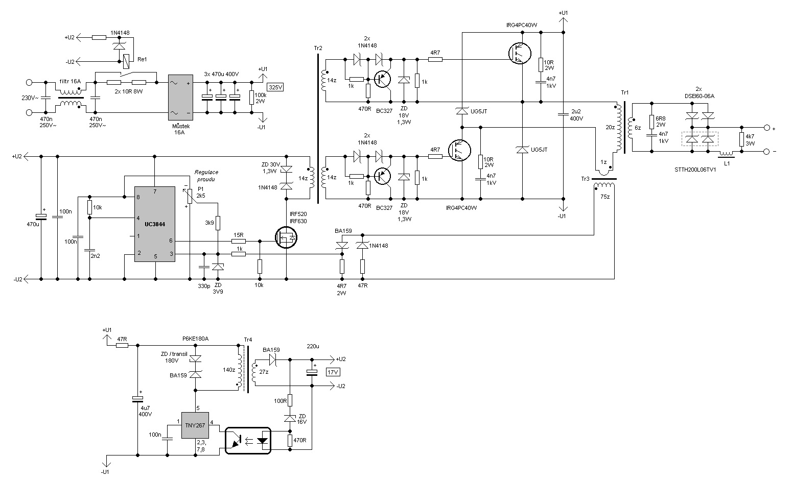
F1 on the first schematic is 0.5A/250v. This means the max sustained current through these big traces is really only 0.5A - either the fuse value is wrong, or that part of the circuit really only uses that much current. Is this a vetted design? Has someone built this, and it actually works? Unless you saw it with your own eyes, be very dubious.
UC3842 is a PWM controller. It can do 500kHz max, not 2MHz.
TR1 and TR3 are very special transformers. If there are no part numbers or instructions on exactly how to make them, this circuit will not work.
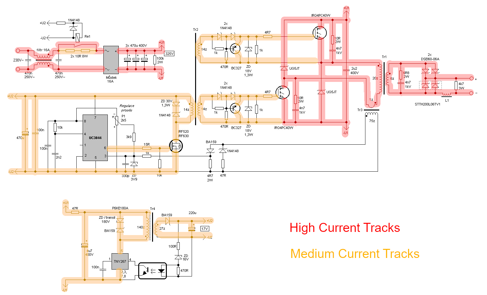
Consider the following annotated schematic for anticipated track widths. Red needs to be 600mil, even bigger on TR1 output. Orange needs to be fairly beefy, perhaps 30mil. Everything else can be small, such as 10mil.

Edit: UC3842 should have medium tracks to pins 7 and 5 also.


