2
\$\begingroup\$

I'm using a Lattice spreadsheet view inside of Diamond with a MachXO2-256-HC-4TG100C. When I assign pin 18 to a port on my design, I get an error:

ERROR - The pin [18] is not user assignable and cannot be assigned to the port [clk_sel_in]; for details, please refer to the device datasheet.

  • phys pin on board is connected to slide switch, gnd on one side, n/c on other side, pulled up in fpga.
  • datasheet says pin 18 is just PL7B on Bank 1
  • there are no special functions associated with the pin.
  • all special functions (except JTAG) are disabled just in case in global preferences
  • I don't see any asterisks anywhere in DS1002 for the pin/package.
  • Other datasheets / docs I've checked TN1199, DS1035, TN1204, DS02056, Design Planning Guide, Diamond Users Guide.

I've only used one lattice on one other project so very possible I'm doing something silly or don't understand something about how they do things. Does anyone know what may cause this? I'm using Lattice Diamond 64-bit on Windows version 3.11.2.446. Thanks in advance.

\$\endgroup\$

1 Answer 1

4
\$\begingroup\$

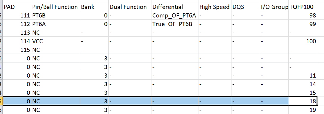
The pinout files for your device can be found here. Based on the "MachXO2-256 Pinout" document, looking at the TQFP 100 package ("TG100" from part number):

Table Excerpt

We see that Pin 18 is a No-Connect pin.


Looking further, did you read "18" from the "PAD" column? (That would be PL5B). That corresponds to pin 17 of the TQFP package, not pin 18.

Excerpt from table

\$\endgroup\$
4
  • 1
    \$\begingroup\$ Just a little addition to this elaborated answer: one can use the "Package View" in Lattice Diamond to get an overlook about all pins, their properties and assignments. \$\endgroup\$ Commented Apr 20, 2020 at 18:12
  • \$\begingroup\$ Thank you for the explanation. I was confusing the pad number with the pin number. RIP to this PCB and on to rev B, lesson learned... \$\endgroup\$ Commented Apr 20, 2020 at 19:57
  • \$\begingroup\$ @SparkyMcSparkface we've all been there. Best advice I can offer is to test compile your pinout before committing to PCB. \$\endgroup\$ Commented Apr 20, 2020 at 21:24
  • \$\begingroup\$ @SparkyMcSparkface you could place a solder bridge between 18 and 17 if 18 is really a NC. \$\endgroup\$ Commented Apr 21, 2020 at 6:55

Your Answer

By clicking “Post Your Answer”, you agree to our terms of service and acknowledge you have read our privacy policy.

Not the answer you're looking for? Browse other questions tagged or ask your own question.