0
\$\begingroup\$

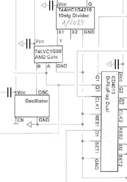
On my prototype board I used an integrated oscillator which gave me the desired frequency without any extra component. Then it's being divided by a divider ic. The clock pulse going from the oscillator to the 8 stage divider 74AHC1G4208 is turned on and off by an AND gate. The ON-OFF signal comes from a D Flip-Flop CD4013. On the prototype I use a 10 stage divider. But in the final version I will use a 8 stage divider, which is the same. So I linked to the 8 stage version of the chip.

enter image description here

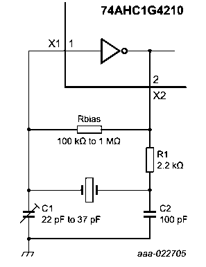
This circuit works perfectly. Now that I plan production in some quantity, I would like to replace the oscillator ic by a much cheaper and also more available, crystal and its passive components, as shown on this schematic from the divider ic 74AHC1G4210 datasheet. This chip has an built-in output X2 for oscillator circuit. X1 is the clock input being divided. I plan to copy this circuit.

enter image description here

The crystal is an IQD 4.9152 MHz.

Could you tell me how I can turn this circuit on and off as I did with the AND gate. If I put an AND gate between the crystal and X1, I imagine it won't work because the AND gate will prevent resonance with the crystal.

Maybe I could sink the current coming from X2 to the crystal, limited by R1 (in this case 4.7K or 10K) with a N-MOSFET? But wouldn't that perturb the crystal?

The first 5 or 6 pulses can be irregular, as long as the next ones are at the good frequency.

I also have no idea what value should be for Rbias, C1 and C2, except from the indication on this schematic. It reads: "R1 is the power limiting resistor, its value depends on the frequency and required stability against changes in VCC or average ICC. For starting and maintaining oscillation a minimum transconductance is necessary, so R1 should not be too large. A practical value for R1 is 2.2 kΩ."

\$\endgroup\$
5
  • \$\begingroup\$ Could you instead disconnect the output from the next stage, perhaps using a small FET? Effectively this turns off the clock signal from the view of any downstream components. It also has the benefit that your clock source remains stable. \$\endgroup\$
    – David
    Commented Apr 30, 2020 at 22:54
  • \$\begingroup\$ Perturbing this Xtal oscillator may be a bad idea...crystals are high-Q which means that their oscillating amplitude changes slowly with time. It takes many, many cycles to stabilize. \$\endgroup\$
    – glen_geek
    Commented Apr 30, 2020 at 23:28
  • \$\begingroup\$ If you're running at 3.3V, you might be able to use a low threshold PFET like the NX3008PBKW to turn off the connection between X2 and R1/Rbias. You would also have to add a resistor of the same order as Rbias to pull the X1 input to ground when the PFET gate was at 3.3V. \$\endgroup\$
    – crj11
    Commented May 1, 2020 at 0:02
  • \$\begingroup\$ Why don't check your smart phone mainboard for solution. So you will be see more analog switching ic's. And you can't divide frequency like this, got stability problems. Use an FPGA or CPLD, maybe you can success but never create an feedbak point ! \$\endgroup\$
    – dsgdfg
    Commented May 1, 2020 at 0:30
  • \$\begingroup\$ @crj11 That's a solution to explore, on top of the other answers. The biggest problem it seems, is the delay it takes to stabilize the pulse between each enable/disable cycle. \$\endgroup\$
    – Fredled
    Commented May 1, 2020 at 15:13

2 Answers 2

2
\$\begingroup\$

Could you tell me how I can turn this circuit on and off as I did with the AND gate.

You could feed the enable signal into the X1 pin through a diode (eg. 1N4148) with Anode to X1 so it pulls down to ground and turns the oscillator off when low, but doesn't affect it when high.

The first 5 or 6 pulses can be irregular, as long as the next ones are at the good frequency.

Without knowing the exact requirements of your circuit I can only say that crystal oscillators take a long time to the start up, so if you try to turn the oscillator on and off directly there will be a lot more disturbance than just 5 or 6 'irregular' pulses. There could be a delay of tens or hundreds of milliseconds before the oscillator level builds up enough to clock the divider reliably.

Since your existing circuit works, I suggest using a separate Gate IC (eg. 74LVC1GU04) for the oscillator.

\$\endgroup\$
7
  • \$\begingroup\$ Using the enable signal at X1 is a good idea. I can pull it up or pull it down. But if it takes that long to rebuild a stable pulse, it's not good. The pulse can be irregular for a few microseconds, not a few milliseconds, Maybe it needs testing. I'm surprised it takes so long. \$\endgroup\$
    – Fredled
    Commented May 1, 2020 at 15:09
  • \$\begingroup\$ You suggest I make a complete circuit with an inverter instead of X2? \$\endgroup\$
    – Fredled
    Commented May 1, 2020 at 15:18
  • \$\begingroup\$ Do you think I could use the AND gate instead of the schmitt trigger inverter (circled in red) in this circuit: electronics.stackexchange.com/questions/218142/… \$\endgroup\$
    – Fredled
    Commented May 1, 2020 at 15:37
  • \$\begingroup\$ You can use a SN74LVC2GU04DBVR, which is a dual unbuffered inverter. Use half to duplicate the oscillator circuit in the existing circuit. Feed the output of the oscillator inverter to the input of the second inverter through a ~100K resistor. Pull the 100K resistor high or low at the inverter input to disable the clock and disable the driver to allow the clock to run. If you synchronize the on/off of the driver disable with the clock, you can avoid glitches during the transition. The clock from the first inverter is always running, it is just stopped at the input to the second inverter. \$\endgroup\$
    – crj11
    Commented May 1, 2020 at 17:13
  • \$\begingroup\$ For most reliable operation of the oscillator you should use an unbuffered gate, since this works better as an analog amplifier. I strongly advise not using tricky circuits in an attempt to reduce the component count. SOT23 gates are small enough and cheap enough that you shouldn't have to risk compromising the design. \$\endgroup\$ Commented May 1, 2020 at 17:21
2
\$\begingroup\$

This type of oscillator is called a Pierce Oscillator.

Could you gate the oscillator signal after the eight stage divider, if you could live with the first pulse after the oscillator is enabled being an odd length? Failing that you could use your own NOT gate to build the oscillator. Gating then possible. This enable/disable gate should be a schmitt Nand to square up the oscillator's output because Rbias biases the NOT gate into the linear region.

C1 & C2 would be chosen so that CL (the total load capacitance) on the crystal is 18pF, the data sheet recommended value. The total load capacitance on the crystal is made up from C1, C2, the input and output capacitances of the inverter + strays. Using a value for CL away from the recommended load capacitance will pull the crystal off frequency.

Using the standard equation for calculating a CL of 18pF requires C1 = C2 = 27pF. A ball park figure for the input and output capacitances of the inverter would be 5pF and stray capacitance could be taken to be 2pF. Then using this equation.

Equation

As a rule of thumb R1 should have a value equal to the reactance of C2 at the oscillator's frequency.

R1 = 1/(2 * pi * 4.9152M * 27pF) = 1k2

Once built you would need to check that it functions correctly over a range of temperatures.

\$\endgroup\$
1
  • \$\begingroup\$ No I can't gate after the divider. Unfortunately. Thanks for the explanations with the formula. I'll be back when I figure all that out. \$\endgroup\$
    – Fredled
    Commented May 1, 2020 at 14:54

Your Answer

By clicking “Post Your Answer”, you agree to our terms of service and acknowledge you have read our privacy policy.

Not the answer you're looking for? Browse other questions tagged or ask your own question.