More than a month has passed since this question was asked and probably it is no longer attractive either for the OP or for those who are interested in building reputations. But still I decided to write this answer because I have long been impressed by the ingenious simplicity of this idea...
"However, what I don't understand is why there is a resistor at the top (and why its input is set to High) and how this results in a High output for the entire circuit."
This logic gate is based on the NMOS inverter (aka switch) which in turn is based on the common-source amplifier stage. The role of the drain resistor Rd can be explained in a few ways and all will be true. Some of them actually "explain" nothing ("Rd is the drain resistor"). Others are formal ("Rd acts as a current-to-voltage converter") or too primitive ("Rd is a current-limiting resistor"). There are brilliant intuitive ("Rd and the transistor form a dynamic voltage divider") and figurative explanations ("Rd is a pull-up resistor")... but, as a rule, all they explain specific circuit solutions...
With my intuitive explanations below I will try to reveal the philosophy behind the various specific stage topologies. I will do it in the form of a fictional circuit story; so do not consider the written as absolute truth.
The problem. In the simplest logic gate (inverter or follower), the input voltage has to change the output voltage (Fig. 1) between two extreme values - Vdd (logical 1) and zero (logical 0). So, the question is, "How do we do it?"

Fig. 1
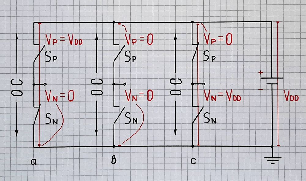
Connecting/disconnecting ideal voltage sources through ideal switches. The obvious way (Fig. 2 and Fig. 3 below) to do this is to connect through switches the output either to Vdd (logical 1) or to ground (logical 0). As though there are two voltage sources - a Vcc voltage source and a "ground" voltage source with zero voltage… and the input voltage determines what of them to be connected to the common output. This circuit works fine in the steady state ("a" and "d" cases) but problems appear during the transition ("b" and "c" cases). Let's see why…
"Open circuit" problem. We (the input voltage source) can change the output voltage (e.g. from zero to Vdd) in two ways. For example, we can first open the closed switch and then close the open switch, i.e. we first disconnect the active voltage source and then connect the inactive source (Fig. 2b). But the problem is that during a short time interval both switches are open (both voltage sources are disconnected). As a result, the output is "floating" (undefined)... and this is undesired in this case.

Fig. 2 (OC = "open circuit")
"Short circuit" problem. With the same success, we can first close the open switch and then open the closed switch, i.e. we first connect the inactive voltage source and then disconnect the active source (Fig. 3b). But now another problem appears - during a short time interval both switches are closed (both voltage sources are connected to the output). This means a short circuit... that is also undesired.

Fig. 3 (SC = "short circuit")
How do we solve these problems?
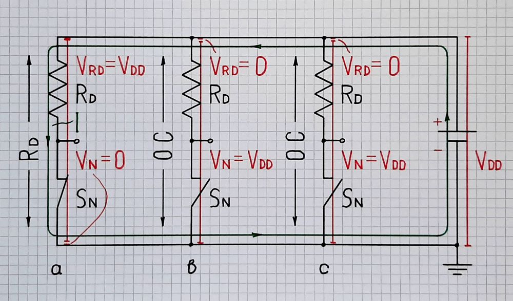
Connecting an ideal to real voltage source through an ideal switch. In the beginning of the transistor era, they solved these problems by a simple electrical trick. They used the fact that if an ideal voltage source is connected in parallel to a real voltage source, the common voltage across both sources is equal to the voltage of the ideal voltage source. Thus the ideal voltage source automatically "disconnects" the real voltage source and imposes its voltage on the output without the undefined "open circuit" state and dangerous "short circuit" state.
To implement this idea, they converted the "ideal" voltage source Vdd into a real voltage source with internal resistance by adding the resistor Rd in series to the power supply (Fig. 4).

Fig. 4
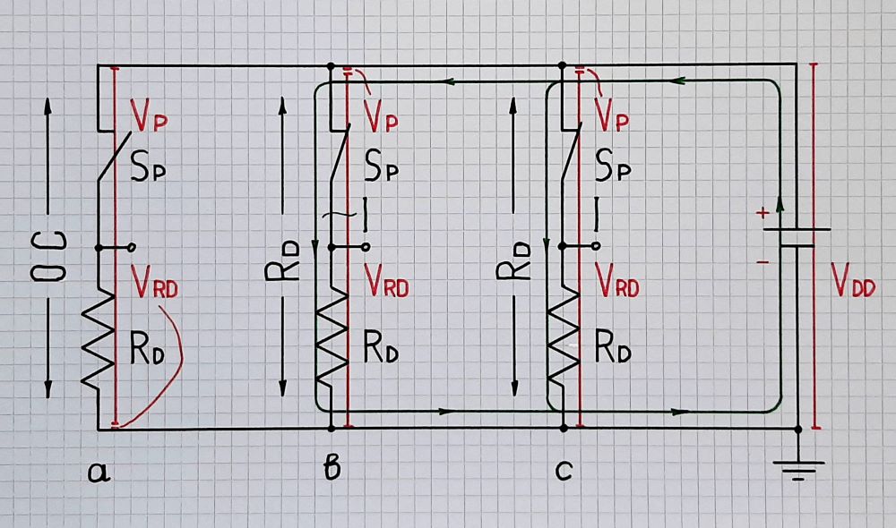
With the same success, the "ground voltage source" can be converted into a real voltage source by adding a resistor Rd in series to the "ground source" (Fig. 5). The first version is implemented by an N-channel MOSFET and the second version by a P-channel MOSFET.

Fig. 5
The problem of this 1-transistor solution is the relatively high output resistance in one of the two states. It is entirely determined by the resistance Rd.
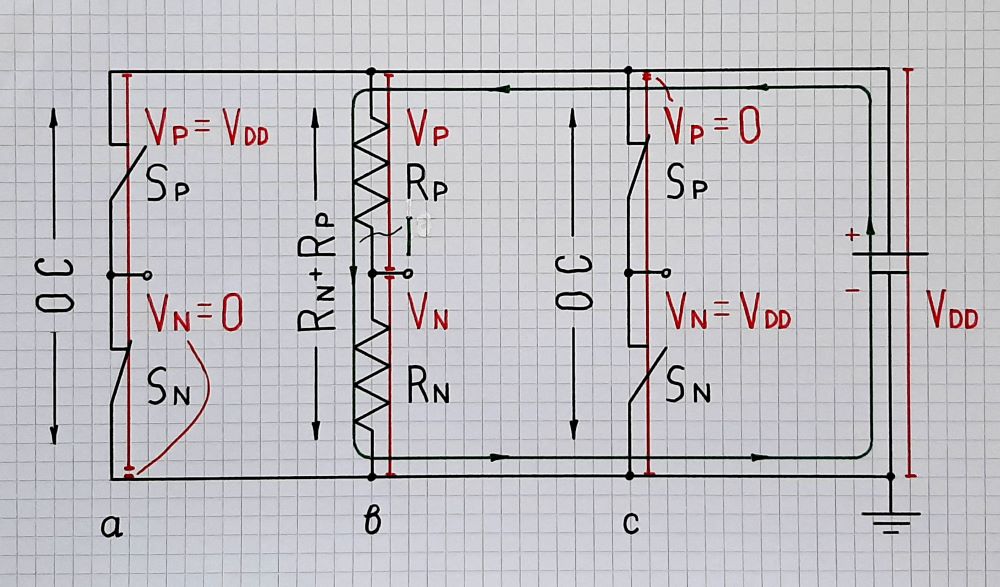
Connecting/disconnecting ideal voltage sources through switches with "dynamic" resistance. We need the resistance only during the transition to limit the current through the network; in the steady state, the resistance is undesired - Fig. 6. So, it has to be dynamic - moderate during the transition (Fig. 6b) and zero during the steady state (Fig. 6a and 6c).

Fig. 6
This idea is implemented in an elegant way in the ubiquitous complementary pair of NMOS and PMOS FETs (CMOS). Their transfer characteristics overlap in the middle so the voltage is fixed at Vdd/2 and the current is limited to Vdd/(Rn + Rp).
Disconnecting the circuit from the load. As we noted above, when both switches were open, the output was "floating" - Fig. 2b. There this state was undesired since the input voltage of the next stage was undefined. But in computers this is an extremely useful circuit trick that allows to connect/disconnect CMOS devices to/from computer buses. It is known as a "3-state output", "high-Z output", etc...
This was my amazing story dedicated to MOS and CMOS inverters that I wanted to hear from my teachers in the late 70's. I just wanted them to explain to me in simple human words not only what is done but why this was done that way. And since that did not happen, I did it myself now.


