1
\$\begingroup\$

enter image description here

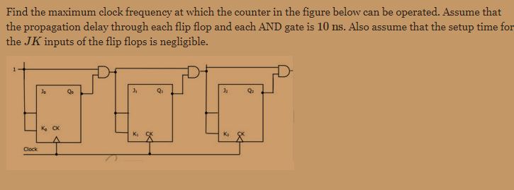
My Doubt is that, This is synchronous counter, all the flip-flop are activated simultaneously Right?

Suppose at t=0 clock is activated then j0 and k0 will be activated instantly but my doubt is that in this time what will be the content of j1 and k1 or j2 and k2 does they have previous value i.e value they contain in previous clock cycle? Right? Okay now t=0 j0 and k0 will output qo complement this will reach AND gate and after 10 ns they will reach j1 and k1 right? Does my understanding is correct? Please help me to visualize how to calculate delay. Somewhere i read we taking only maximum delay I'm all confused here Please help.

\$\endgroup\$
1

3 Answers 3

0
\$\begingroup\$

My Doubt is that, This is synchronous counter, all the flip-flop are activated simultaneously Right?

Right

Suppose at t=0 clock is activated then j0 and k0 will be activated instantly but my doubt is that in this time what will be the content of j1 and k1 or j2 and k2 does they have previous value i.e value they contain in previous clock cycle?

if you mean t=0 when power is first applied, then the output is random (undetermined) depending on the race between the internal gates of the flip-flop. We can force the initial value by external components but it is not related to this question.

now t=0 j0 and k0 will output qo complement this will reach AND gate and after 10 ns they will reach j1 and k1 right?

Q0 will change on the clock positive edge and the output of the AND gate will be guarantied to be as expected after 10 ns and stable.

to find out the maximum clock frequency you must take into consideration that after any clock edge, the next clock edge must not arrive before all the AND outputs are stable including the last one although it does not affect the operation but at the end the output is here to be used (so after the input is stable and the output is stable on each one).

\$\endgroup\$
0
\$\begingroup\$

Your understanding is partially correct:)

Let's clarify a few points step by step. Yes, this is a synchronous counter. This means all the flip-flops are clocked simultaneously. The clock input of all the flip-flops is connected to a common clock signal. At any time t, the inputs J1, K1, J2, K2, etc., indeed hold the values they were last provided with. If you've just started up the system and haven't provided any inputs, the flip-flops might be in an undefined state (often referred to as a metastable state). At t=0 when the clock signal goes high, J0 and K0 will indeed be activated instantly. When Q0 changes (because the JK flip-flop toggles), this change in Q0 will take time to propagate through the AND gate and then will take additional time to affect the next flip-flop. Propagation through AND Gate - this will indeed introduce a delay of 10ns as per the given information. The output of the AND gate will reach J1 and K1 after the AND gate's propagation delay. For synchronous counters, while all flip-flops receive the clock signal simultaneously, the change in state of one flip-flop might affect the behavior of the next due to the combinational logic (like the AND gate) in between them. This logic introduces delay. The delay through each flip-flop and AND gate is 10 ns. Thus, the total delay from the clock edge until J1 and K1 see the effect is 20 ns (10 ns for Q0 to change + 10 ns for AND gate).

So: To find the maximum clock frequency, you'll take the inverse of this total delay. Max frequency = 1 / Total delay = 1 / 20ns = 50 MHz.

When you're dealing with synchronous digital systems, and you want to determine the maximum operating frequency, you often consider the 'worst-case' or 'maximum' delay scenario. This ensures the system operates reliably under all conditions.

I hope this helps clarify the problem.

\$\endgroup\$
1
  • \$\begingroup\$ Undefined is not the same as metastable. For instance, after application of power and in the absence of any clocks, the Q outputs of each flip flop will be stable, but, but you don't know if it will be a 1 or a 0. \$\endgroup\$
    – SteveSh
    Commented Mar 18 at 2:10
0
\$\begingroup\$

First, the drawing's a bit confusing. I infer that the J and K inputs are tied together ('J' label isn't lined up.)

That out of the way, you need to identify the critical path. That is, find the path that has the longest cumulative delay from clock to a flop input.

Yes, you are correct that all the flops change state together. But that's not the whole story.

Hint: notice the first two AND gates. They're connected head-to-tail so their delays add together to the input of the third Q2 flop. Let's call them AND1 and AND2. By inspection, together with Q0 clock-to-Q they are the critical path.

So we have:

  • Tcq Q0 (leftmost flop) = 10ns
  • Tpd AND1 = 10ns
  • Tpd AND2 = 10ns
  • Tsu J/K 2 (rightmost flop) = 0ns

These add up to 10 + 10 + 10 + 0 = 30ns. This gives us a max frequency of 1/30ns = 33MHz.

(And Dave Tweed came to the same conclusion when he saw this some years ago. 30ns it is.)

\$\endgroup\$

Your Answer

By clicking “Post Your Answer”, you agree to our terms of service and acknowledge you have read our privacy policy.

Not the answer you're looking for? Browse other questions tagged or ask your own question.