0
\$\begingroup\$

I am trying to switch a 17VDC 30mA load with a Raspberry Pi. To provide electrical isolation, I am using a two channel optocoupler, a TLP621-2 (datasheet). The second channel is currently unconnected.

My understanding is that I can't drive the optocoupler directly from the 3.3 VDC GPIO pin on the Pi because the pin can only source/sink 16mA. So I'm using a 2N3904 transistor to control the LED in the optocoupler. Putting 17VDC 30mA on the coupler's outputs isn't wise either so I have a second transistor there as well.

The problem is that I don't know how to complete this circuit? I've tried different permutations on the output and can't get it to switch the load. I have no idea whether I have things hooked up incorrectly or I keep smoking ICs (or both?). The input transistor seems to switch as expected when I apply 3.3V to it's base, so I assume that the coupler's LED is activated. But nothing happens on the output. I'm wondering if I'm misunderstanding the TLP621's datasheet?

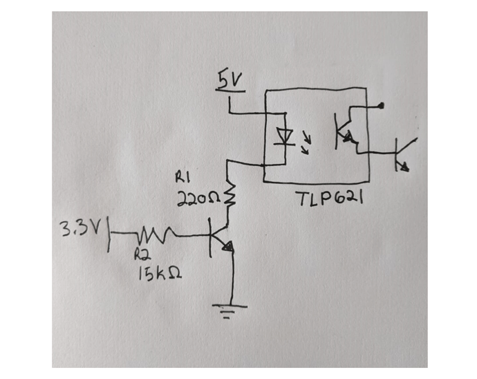
TLP621 schematic

\$\endgroup\$

2 Answers 2

1
\$\begingroup\$

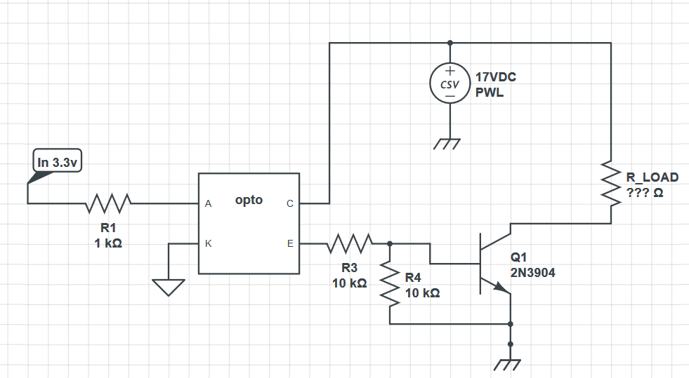
You don't have to bother the poor opto-coupler with an overload pressure. Also, you can drive the opto with RasPi's GPIO easily with a low current. At its output there would be also a low current which is enough to drive a BJT. So the BJT is the one who switches the load.
Try this circuit:

enter image description here

\$\endgroup\$
0
\$\begingroup\$

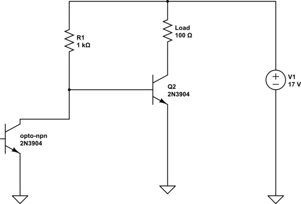
Check the schematic below:

schematic

simulate this circuit – Schematic created using CircuitLab

When opto transistor is ON, external transistor's base gets grounded and it is turned OFF which turns OFF the load as well.

When opto transistor is OFF, external transistor turns ON due to pull up resistor R1. This turns the load ON.

\$\endgroup\$
3
  • \$\begingroup\$ The worst case current transfer ratio is 50% so with less than 20mA into the LED the maximum guaranteed output current that can be designed for is ~10mA. The 30mA will require a buffer on the output side. You could run the LED at only 5-10mA and so not require the input side buffer. \$\endgroup\$ Commented Jun 20, 2020 at 16:47
  • \$\begingroup\$ @kevin - thanks for pointing that out. Edited my answer. \$\endgroup\$ Commented Jun 20, 2020 at 16:53
  • \$\begingroup\$ Thank you for the answer. I'm having difficulty understanding your schematic though. It looks like you have the output transistor (pins 7 and 8 on the TLP621-2) labeled as a 2N3904? Why is the 100 ohm resistor labeled as "load?" Should the components be connected as VCC --> load --> 100 ohm resistor --> collector? Sorry, but I'm still trying to learn how to use transistors. \$\endgroup\$
    – jamieb
    Commented Jun 20, 2020 at 18:34

Your Answer

By clicking “Post Your Answer”, you agree to our terms of service and acknowledge you have read our privacy policy.

Not the answer you're looking for? Browse other questions tagged or ask your own question.