Introduction
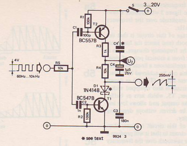
To find out the limiting factors, I carried out spice simulation of the above circuit.
- The results seemed dependent on the software used.
- Moreover, the limits given by the author (viz, 60Hz and 10kHz) looked like general suggestion rather than a hard limit beyond which the output drastically changes.
- Moreover, the result also is quite sensitive to the differentiator circuits and the BJT model parameters.
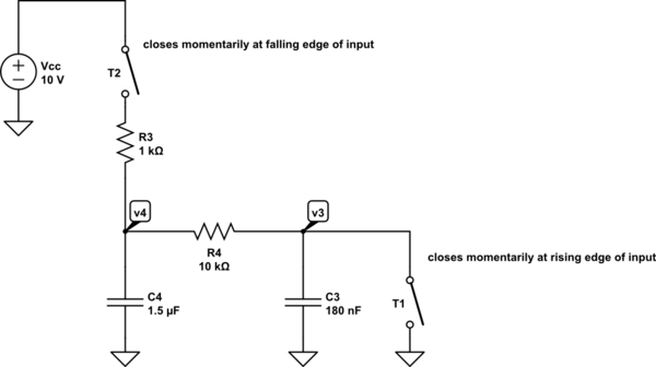
- A highly simplified model can reproduce the spice results. Only C4, C3, R3, R4 are required to explain the limitations of the circuit.

simulate this circuit – Schematic created using CircuitLab
Simplified circuit
The components R1, C1, R2, C2, T1, T2, R5 are all absorbed into the ideal switches conveniently named T1 and T2. T1 and T2 are momentarily closed for a small duration at rising and falling edges of the input respectively. C4 is neglected as it is not fully necessary to explain the circuit as the author themselves mention.
Sometime after a falling edge, T2 becomes open. Till next falling edge C4, R4 and C3 are in series (except for brief moment during rising edge when T1 also closes).
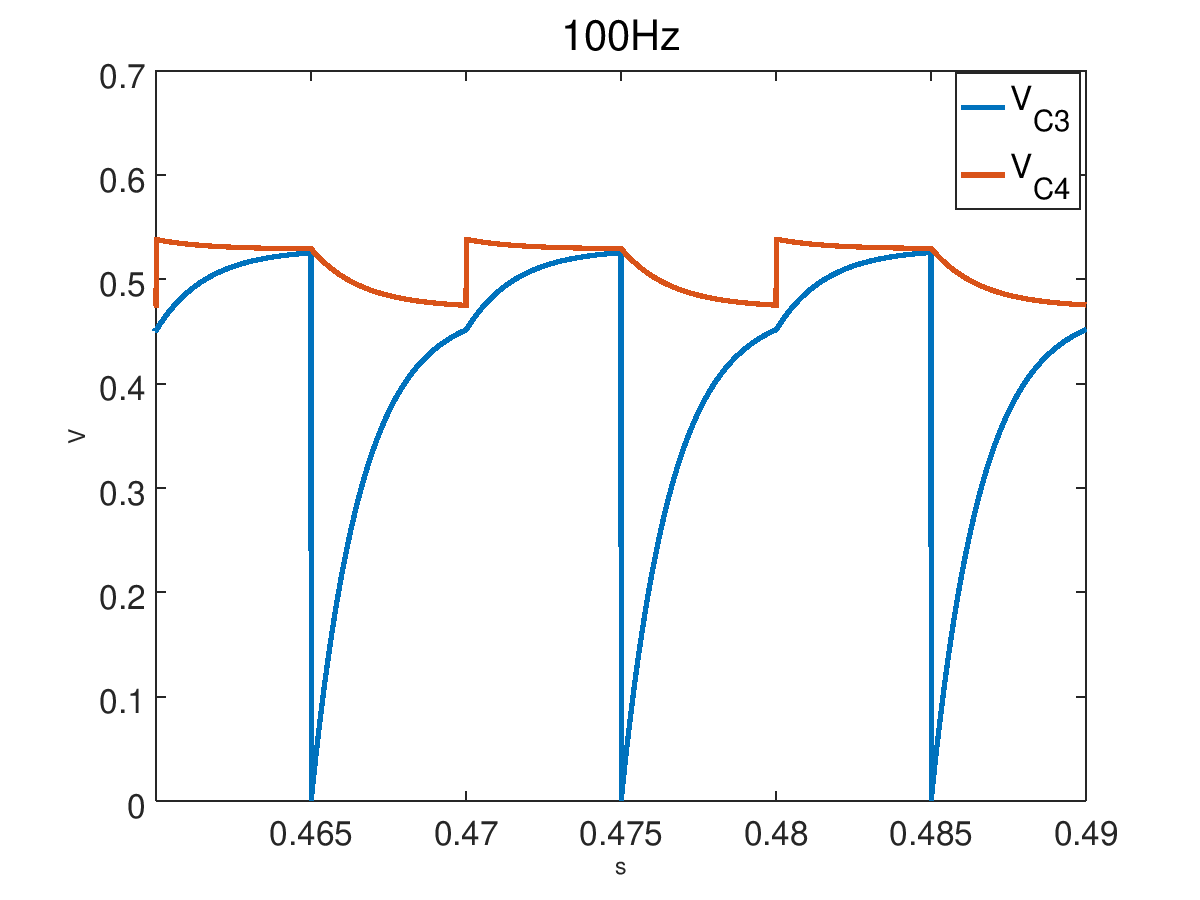
We can also note that the discharge of C4 through R4 into C3 has only a small effect on its voltage since C3 is 8.33 time smaller than C4. The voltage of C4 is also not much affected by closing of T1 since the discharge is through a 10k resistor (C4 is later re-charged quickly through the 1k resistor).
At lower frequencies
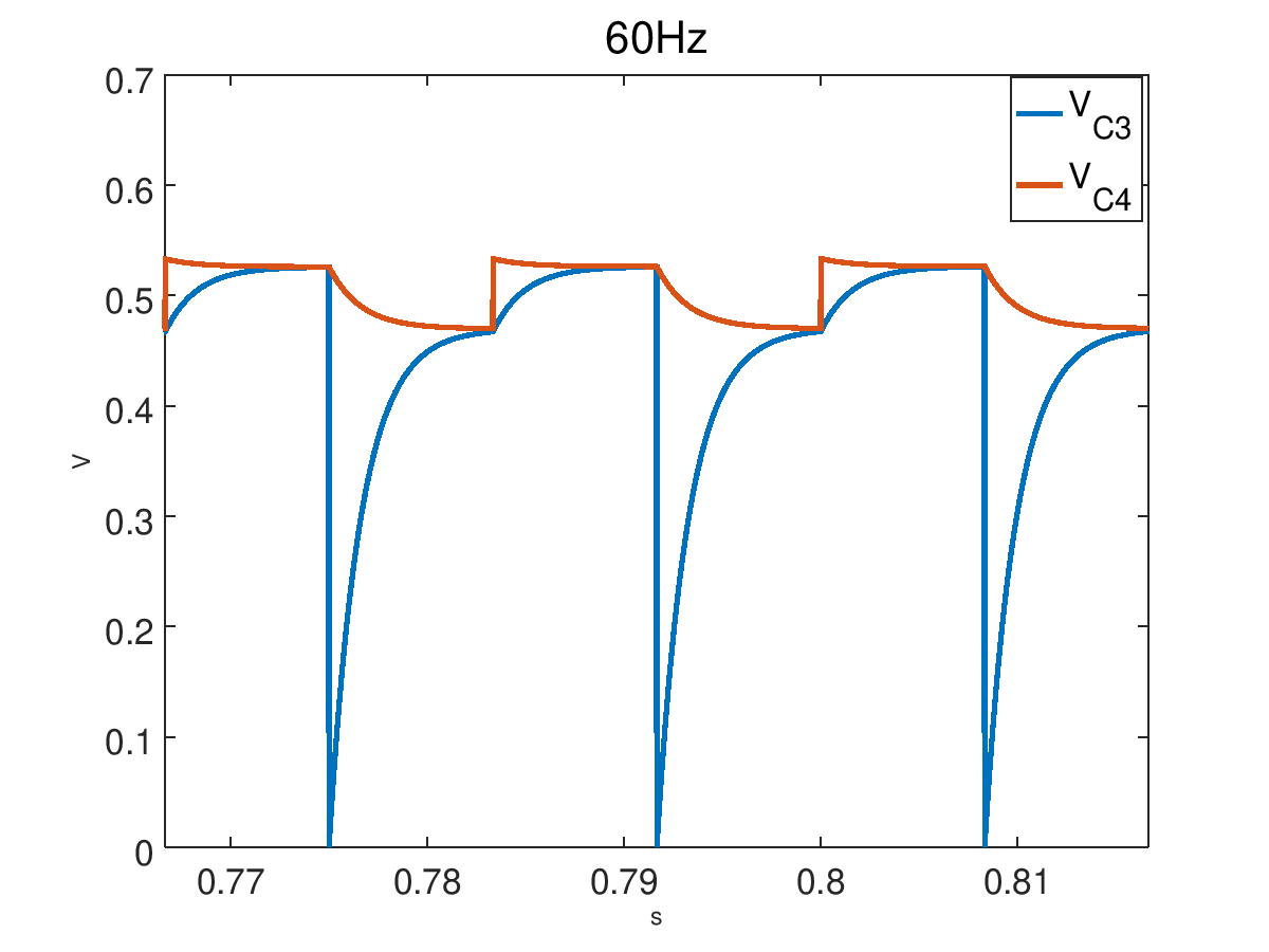
Consider both switches open. C3 is charging via R4 from the voltage provided by C4. C4 can be approximated as a constant voltage source since C4 is 8.33 times larger than C3. So the time constant of this charging is R4C3 = 1.8ms. We can say that C3 will reach very close to its final voltage by about 5 time constants; i.e. within 9ms. So if the input frequency is less than 1/9ms = 111 Hz, then the output of C3 will no longer look like a ramp, but more like a square wave with smooth corners. The response* for 100 Hz shown below illustrates this well. The 60Hz quoted by the author corresponds to nearly 10 time constants. The assumption that C4 is nearly constant voltage is also justified by the figures.


At higher frequencies
At higher frequencies also the C3 charges via R4. The ramp voltage is given by
\$V_3(\tau) = V_4 (1 - e^{-\tau/(R_4 C_3)})\$
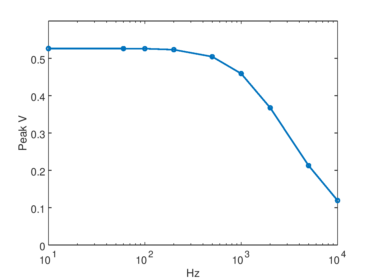
To reach a peak ramp amplitude of \$V_{3peak}\$, the voltage of C4 should have had risen to \$ V_4 = V_{3peak}/(1 - e^{-\tau/(R_4 C_3)})\$. The time \$\tau\$ is slightly less than the time period of the input signal, since, after one period of the input signal, C3 is discharged to zero volts. As input frequency increases, \$\tau\$ decreases and the required charge on the capacitor C4 goes above the supply voltage (which is not possible for this circuit). Again, here also the upper limit suggested by the author may be general suggestion rather than a strict limit. the ramp amplitude drops off gradually as frequency increases. Figure shown below.

Addendum
To illustrate that the above simplified model only is required to model the lower and upper limits on the frequencies, the voltage waveforms shown above are actually generated from differential equations for the simplified circuit rather than a spice model.
