3
\$\begingroup\$

as you know for a BJT in active region we have

\$i_C=\beta\cdot i_B\$

\$i_B=I_S \cdot e^{\frac {q\cdot v_{BE}}{kT}}\$

So, if you suppose that the base-emitter voltage is set by a voltage source:

  • Collector current is linear with respect to the base current;
  • Base current is not linear with respect to the base-emitter voltage;

The last one may be approximated as a linear function of only a small input signal which is applied in addition to a biasing voltage.

Since in amplifiers, for instance, non-linearity are not so good, I was asking me: why do not we use always current signal sources for a BJT amplifiers? In this case we would simply write:

\$i_c=\beta\cdot i_b\$

where \$i_b\$ is our signal, and so we have bypassed the problem of non-linearity.

\$\endgroup\$
4
  • \$\begingroup\$ To resolve this issue, we add an emitter resistor to keep DC base current constant and then use the AC emitter voltage to modulate the AC current with less gain (=Rc/Re) but more linearity, or we use negative feedback which lowers impedance and less voltage gain (~70% Rf/Rin) but gives the best linearity. \$\endgroup\$
    – D.A.S.
    Commented Jun 28, 2020 at 4:22
  • 4
    \$\begingroup\$ Because \$\beta\$ isn't predictable. It varies from device to device within a family, varies over operating temperature, varies with respect to collector current (though more so at the extremes, I admit), drifts over time, etc. Better to operate it as an emitter follower (they call it emitter degeneration but it's really also just operating it as an emitter follower) that creates a nice, clean, predictable linear current vs input voltage. \$\endgroup\$
    – jonk
    Commented Jun 28, 2020 at 4:28
  • \$\begingroup\$ (1) Most signal sources are voltage (2) converting a voltage source is complicated (3) running BJTs at maximum beta produces totally undesirable temperature/Beta problems (4) running with an emitter resistor solves this. \$\endgroup\$
    – Andy aka
    Commented Jun 28, 2020 at 7:56
  • \$\begingroup\$ You might check this answer: electronics.stackexchange.com/a/497821/152483 . Although it is about MOS transistor, the principle is the same: smaller sensitivity. \$\endgroup\$ Commented Jun 28, 2020 at 12:28

4 Answers 4

6
\$\begingroup\$

Not a full answer, but a contribution to a possibly complete one.
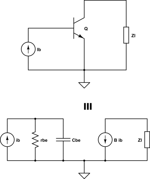
As @Neil_UK alludes in his answer, frequency response is a matter of concern in properly designed amplifiers. To fix ideas, let's consider the simplest common emitter amplifier BJT stage: if you drive it with a high impedance generator, ideally a current source, you are in the following situation:

schematic

simulate this circuit – Schematic created using CircuitLab

The part of the \$i_b\$ current which effectively controls the \$i_c=\beta\cdot i_b\$ current is the one which flows in the base-emitter resistance \$r_{be}\$, which is shunted by the base-emitter capacitance \$C_{be}\$. Thus there is a high frequency pole in the input circuit of the amplifiers which limits the overall bandwidth of the circuit. And now the question is: How this pole influences the global bandwidth?
The value of \$r_{be}\$ could be (and usually is) in the \$\mathrm{k}\Omega\$ range, while in the data sheets you see a \$C_{be_o}\$ which is of the order of few \$\mathrm{pF}\$ (or less): so why this pole should concern us?
This is because the real capacitance of the input of the BJT is far larger: precisely, $$ C_{be}\simeq C_{be_o} + \frac{\mathrm{d} Q_{b}}{\mathrm{d} v_{be}}\label{1}\tag{1} $$ where \$Q_{b}=\tau_b\cdot I_c\$ is the total base charge. The second term on the right side of the expression \eqref{1} has the following form $$ \begin{split} \frac{\mathrm{d} Q_{b}}{\mathrm{d} v_{be}} &\simeq \tau_b \frac{\mathrm{d} I_{c}}{\mathrm{d} v_{be}} = \frac{\tau_b I_{EB}}{V_T} e^\frac{v_{BE}}{V_{T}} \\ &\simeq \tau_b g_m v_{be}\; \;\text{ if } v_{be} \text{ is "small"} \end{split},\label{2}\tag{2} $$ where

  • \$\tau_b\$ is the base minority carrier lifetime,
  • \$I_{EB}\$ is the emitter base junction saturation current
  • \$g_m=\frac{I_C}{V_T}\$ is the BJT forward transconductance.

When the BJT is biased in forward active region, the common values of the listed parameters are such that \eqref{2} is the dominant term in \eqref{1}: this implies that the base circuit of a common emitter BJT amplifier has a very slow frequency response when driven by an ideal current generator, and this limits the overall frequency response of the amplifier in an essential way. Note also that the capacitance \eqref{2} is highly nonlinear, thus the bandwidth response is low and decreases as the input voltage increases, thus making the also the low distortion goal vanish.

Conclusions

  • The frequency response of a BJT driven by an ideal current source is severely limited by the structure of the input pole of the BJT itself. Thus the relative linearity of the gain is usable only at low frequencies. If you drive the same BJT with an ideal (in practical a low impedance) voltage source, then \$r_{be}\$ is (almost) short circuited, thus the frequency response of the input circuit can be vastly improved.
  • The input capacitance of a forward-active biased BJT is highly nonlinear: as a matter of fact, its main component behaves exponentially respect to the base emitter voltage \$V_{BE}\$. This especially significant in large signal circuits, where it would be also advisable to achieve the best low distortion performance. Thus, even if the relation between \$I_C\$ and \$I_B\$ is nearly linear at DC, as the frequency and the driving voltage rise, a number of frequency dependent nonlinear phenomena will appear, making the linearity advantage of an ideal current generator driving vanish.
\$\endgroup\$
2
  • 3
    \$\begingroup\$ Good answer - gratulation. We can compare the situation with a simple voltage divider: A very large source resistor Rs and comparable small load resistor Rbe, which is shunted with the input capacitance at the base node. A low resistive voltage source (ideally zero source resistance) at the base would create a much smaller time constant and, hence, allow a much larger bandwidth. \$\endgroup\$
    – LvW
    Commented Jun 28, 2020 at 10:12
  • \$\begingroup\$ @LvW exactly. And also the model explains some "strange" characteristics of RF BJTs: their relatively small \$h_{FE}\simeq\beta\$ (usually never above \$100\$) due to the heavy base doping, made in order to reduce \$\tau_b\$. \$\endgroup\$ Commented Jun 28, 2020 at 11:45
4
\$\begingroup\$

We use the simplest model of a transistor that is sufficiently useful for our purposes at any time.

  • \$I_C = \beta \cdot I_B\$ is great for biassing, and for initial teaching,
  • \$i_c = g_m \cdot v_{be}\$ is useful when the transistor is biassed, and we are considering small signals. It results in simpler, more linear equations than the current input model.

There are several important applications that are strictly small signal, for instance noise performance, and stability. Of course, there's amplifying small signals as well.

We need to add stray capacitances to the \$g_m\$ model for any frequency remotely above DC.

We use Ebers-Moll or Gummel-Poon when these models aren't sufficient, to attempt large signal modelling.

When none of the above are good enough, we give up on models and use S-parameters, at a particular bias point.

Recently, one test equipment supplier has begun to try to popularise X parameters, best thought of as an extension of S-parameters to any bias point.

\$\endgroup\$
3
\$\begingroup\$

My answer is simple:

In BJT small-signal amplifiers, we do not control transistors by current since there are significant voltage losses across the internal resistance of the input current source.

As a rule, they are voltage amplifiers; so we have to convert the input voltage to input current. This means to connect a base resistor (acting as a voltage-to-current converter) between the input voltage source and the base. The voltage drop across the resistor is the loss that decreases the stage gain.

Only when applying the input voltage directly to the base-emitter junction, we get a maximum gain. In this case, the maximum input voltage is less than VBE0 (about 0.7 V for Si BJT); i.e., this voltage amplifier has very small input range.

In some cases (e.g., a transistor switch), we need to enlarge it. Then we connect a resistor with relatively high resistance. But in these cases, the transistor is saturated... and this is another story...

These considerations were especially relevant at the beginning of the transistor era, when there were no such sophisticated techniques to artificially increase the gain as a "dynamic load".

\$\endgroup\$
1
\$\begingroup\$

What you are asking for is a CURRENT MIRROR.

You can achieve excellent ratiometric amplification, if the input transistor and the output transistors are

  • of the same doping (they must be near each other, on the same silicon die)

  • of the same temperature (thermal gradients will matter; 1degree C gives 5% mismatch)

  • have the same Emitter voltage (requires attention to "ground" current density, in the aluminum metallization on the silicon)

  • have the same Base voltage (requires attention to distributing the various Base currents)

  • have the same collector_base voltage (and your input transistors will be wired as a DIODE, totally unlike your output transistors, so this requirement is violated)

\$\endgroup\$

Your Answer

By clicking “Post Your Answer”, you agree to our terms of service and acknowledge you have read our privacy policy.

Not the answer you're looking for? Browse other questions tagged or ask your own question.