2
\$\begingroup\$

I would like to measure the voltage of a battery that varies from 4,5V to 3V.

To do so I'm planning to connect this source to a STM32F4 DISCO board and one of its ADCs, which will be set to a VREF+ of 3V. The conversion speed will be very low.

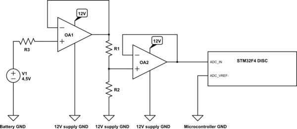
As the voltage from the source is higher than the STM32F4 Vref pin I need to add a voltage divider so that, taking into account I'll use 3V as Vref, the source maximum voltage (4,5V) is converted to 3V, something similar to the following schematic:
schematic

simulate this circuit – Schematic created using CircuitLab

I'm trying to understand how to proceed to have a real measurement voltage value at the ADC_IN if I'm dealing with multiple grounds in the signal conditiong path, Battery GND, 12V GND and Microcontroller GND.

So, I have to main questions:

  • How should I connect the ground nets to have a measurement as accurate as possible?

  • If I have multiple sources to read from and, each source has different ground, could I still have accurate measurements from all sources? How should these grounds be connected?

\$\endgroup\$
12
  • \$\begingroup\$ you could try to use a diff amp referenced to ground per every signal instead and feed its output into MCU ADC, and since it will already be just a difference referenced to ground, there is no need for complicated biasing of Vref. Should work fine unless you have a reason not to use diff amps. Look at some INA180 or something \$\endgroup\$
    – Ilya
    Commented Jun 30, 2020 at 12:08
  • \$\begingroup\$ Thank you very much @Ilya So this would imply adding a shunt resistor between IN+ and IN- of the diff amp, correct? For current measurents I understand that, but in order to measure the voltage from the battery, would I place a high resistance (let's say 10MegOhm) as a Rsense between IN+ and IN- of the diff amp and in parallel to the battery? How should I proceed with that? \$\endgroup\$
    – LazyTurtle
    Commented Jun 30, 2020 at 12:26
  • \$\begingroup\$ nope, just a signal to IN+ and signal's gnd to IN-. And the output will be the difference between them referenced to ground. So if you have a signal of 7V with its ground at 4V to GND (0V), the output will be just 3V. You need to power diff amp from maximum positive voltage you expect as an input (or higher) and ground. Make sure you don't exceed max voltage spec for the IC, pick a sturdy one \$\endgroup\$
    – Ilya
    Commented Jun 30, 2020 at 12:59
  • \$\begingroup\$ Thanks @Ilya but I don't understand, sorry. So, I would connect directly to the battery, IN+ to positivce and IN- to its ground? What will happen if the difference between the source's gnd and the MCU gnd is bigger than 3V (VREF+)? On the other hand, I should connect the diff amp to the MCU's power supply so that its output is referenced to the correct ground, correct? I don't understand why then I have to connect it to a different power supply... \$\endgroup\$
    – LazyTurtle
    Commented Jun 30, 2020 at 13:17
  • \$\begingroup\$ IN+ connects to signal (for example, your signal is 7V). IN- connects to SIGNAL GROUND (say, 4V, so your signal is 3V relatively to its ground potential of 4V). Diff amps power supply are, say, 12V and 0V (I assume 0V is MCU ground). So the output of the diff amp will be just 3V. Your reference voltage for ADC should equal your Vcc, which most likely means leaving Vref floating (check it, maybe connect to Vcc, but usually not, usually it's internally pulled up). So as long as signal magnitude is smaller than Vcc, you're good.If signal range is more, halve the signal.Maybe with voltage divider \$\endgroup\$
    – Ilya
    Commented Jun 30, 2020 at 13:40

2 Answers 2

1
\$\begingroup\$

If you're that concerned about grounds and accuracy, get an instrumentation amplifier like the AD8221: https://www.analog.com/en/products/ad8221.html

This would allow you to do truly differential measurements, and, as a benefit, the datasheet shows you how to set up your bypass capacitors to various supplies and grounds.

You can then use the Vref pin to move the instrumentation amp output to the center of your ADC range.

If you don't need hyper accuracy, I'd probably just tie the battery grounds to the microcontroller ground and then run the V+ terminal into the top of a resistive divider like your R1/R2 (10K/10K or 100K/100K depending upon the required ADC input impedance) above and then run the center directly to the ADC input.

The Beaglebone Black, for example, does this on some of its ADC lines because they are referenced to 1.8V instead of 3.3V.

If you really want to be careful you can probably tie the grounds together through a 100Ohm resistor if you really think you might get weird spikes. A battery probably won't cause any issues like that, though.

\$\endgroup\$
4
  • \$\begingroup\$ Thank you very much for your answer. In my case I'm not looking for super accuracy, but for a minimum conversion quality. Therefore I would like to remove any main possible ground offsets. Regarding to connecting the battery ground to the microcontroller one, wouldn't it be necessary to also connect to these thre the 12V supply ground? And, where should I connect them? As close as possible to the microcontroller? And, regarding the 100Ohm resistor, I might use it as I'm also going to use a linear actuator in the system that would affect this connection. \$\endgroup\$
    – LazyTurtle
    Commented Jun 30, 2020 at 12:37
  • \$\begingroup\$ If you can, connect them all together and give them bypass capacitors. That's perfectly fine. Given that you are testing batteries and not high-speed signals and the currents being tested aren't very high, the grounds really aren't an issue. The linear actuator might provoke some high currents on it's ground. Besides, the ADC on the microcontroller really just isn't accurate enough to get too bent out of shape about ground offset. The input impedance due to it being a delta sigma converter is probably way more than any ground offsets. A 12-bit ADC is only good to about 1mV of accuracy anyway. \$\endgroup\$ Commented Jun 30, 2020 at 12:50
  • \$\begingroup\$ Thank you for your comment. Regarding the bypass capacitor connection, how would you connect them specifically? I don't really understand how this would be done...What I have done several times is connecting the ground in star topology and using an inductor in series with a resistor... \$\endgroup\$
    – LazyTurtle
    Commented Jul 1, 2020 at 10:10
  • \$\begingroup\$ As for the inductor in series with a resistor, we call that passive a "ferrite bead". There are lots of those of various characteristics. As for the the star ground topology, that works really well to isolate things at RF frequencies, but you don't need that here--you are very low frequency and low-accuracy (1mV+). As for bypass, check the datasheet. But generally if you have a +/- 12V part you want to have bypass from +12 to GND, -12 to GND, and +12 to -12. This hits all of the possible return paths. But, again, nothing you've described so far really needs this level of care. \$\endgroup\$ Commented Jul 2, 2020 at 0:39
0
\$\begingroup\$

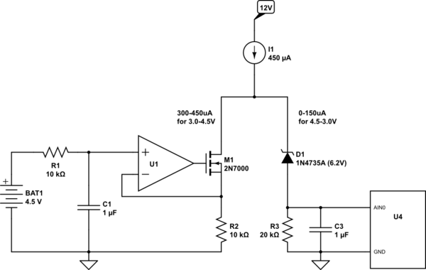
You could use a current to convey the quantity measured between two "ground domains". Have a fixed reference positive current source. Convert the battery voltage into a negative current. The leftover current from the reference is then converted to voltage right at the ADC input pin, using a resistor. Then the ground offsets won't matter much, as long as the compliance of the current sources is not exceeded.

Scaling is done by adjusting the load resistance. Offset is done by changing the reference current. Note that the 3.0-4.5V battery voltage is mapped to 3.0V-0.0V at the ADC input.

The current source I1 would typically be an LM334 configured for 450uA of current. D1's exact value is not critical, it can be 6-10V and is used only to extend the compliance of current source U1+M1 down to "ground" from the point of view of the ADC.

R1+C1 is a 10ms time constant lowpass filter. It ensures that the slew rate of the current source I1 is not exceeded (see LM334 datasheet). C3 smooths out the sampling pulses on ADC's input.

The A/D sampling rate should be kept constant and controlled by a timer, so that the average input current is constant as well. That way the sampling current will cause a constant offset on R3, and not noise dependent on the timing of the software loop that includes A/D sampling.

schematic

simulate this circuit – Schematic created using CircuitLab

\$\endgroup\$

Your Answer

By clicking “Post Your Answer”, you agree to our terms of service and acknowledge you have read our privacy policy.

Not the answer you're looking for? Browse other questions tagged or ask your own question.