1
\$\begingroup\$

I've built a Class C amplifier for educational purposes and believe I understand the major concepts on how it works. The only piece I'm struggling with is how to calculate for the base resistor. From the resources I can find, they authors talk about calculating the RC base network for 10 times the input signal time. My experience is quite different.

The circuit below has the following: Input signal: 11.628 kHz (tuned to the tank circuit) @ 2v p-p Tank circuit: C3 = 213nf, L1 = 877mH Base clamping circuit: C1 = 100uf R = is a variable resistor. I've dialed it to 1.1K ohms, which produces the optimal output p-p signal. The circuit works as expected, but just lost on getting the right math.

My question is: what is the formula to correctly choose the base resistor? Any good resources on negative clamping circuit calculations?

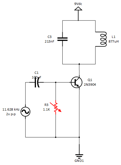
enter image description here

\$\endgroup\$
1
  • 1
    \$\begingroup\$ Your circuit is wrong or your power supply is wrong. Take your pick. \$\endgroup\$
    – Andy aka
    Commented Jul 1, 2020 at 20:51

4 Answers 4

1
\$\begingroup\$

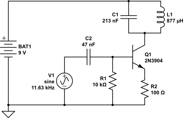
Here's your circuit, ready for simulation.

schematic

simulate this circuit – Schematic created using CircuitLab

Setting C2=100uF, we can sweep R1 from 100 ohm to 1M ohm - we see that not much changes. Its value is non-critical:

enter image description here

But the transistor is driven deep into saturation, as we can tell by the current peaks:

enter image description here

The value that actually matters is that of C2. For C2 <= 10nF, there's no amplification.

enter image description here

But we can now try something between 10nF, where the transistor was cut-off, and 100nF, where it was close to saturation: set C2=47nF, and try with a couple resistor values:

enter image description here enter image description here

The larger the R1, the better the waveform looks, as the transistor is driven with progressively shorter "spikes" that approximate impulse excitation to the tank.

schematic

simulate this circuit

We can now add an emitter load to provide some negative feedback, but that broadens the pulses and makes the distortion worse if you look carefully. So that's a "don't do" for class C. Ideal class C operation is infinitesimally short pulses :)

enter image description here enter image description here

\$\endgroup\$
0
\$\begingroup\$

In that topology all the base bias current is supplied by the source. The base resistor is there to keep the transistor off until enough voltage is available to overcome the Vbe of the transistor. Now in your specific case you also need to adjust the input cap in order to achieve the high pass filter that you are after.

There's lots of info out there if you google a bit.

Class C Amplifiers

Resistor Rb connects to the transistor Q1 base. A biasing resistor which connects to the base of Q1 try to pulls the base of transistor further downwards and set the operating pointer dc bias point below the cut-off point (In cutoff the collector current is ICO which will be of micro amperes order and hence can be assumed to be zero) in the DC load line. The dc load line is the locus of IC and VCE at which BJT remains in active region.

\$\endgroup\$
0
\$\begingroup\$

You may have realized by now you specified an NPN but showed a PNP which is incorrect.

  1. You need to realize that a resonant LC circuit needs a load to be useful and dampen the oscillations so that modulation can occur for Radios. Then a modulation bandwidth must be specified.

  2. Then you need to realize collector current pulses are controlled by Vbe voltage and above ~0.6V the current becomes significant and increases exponentially so Ib must be current-limited to some spec. with a current limiting Rbe determine by the carrier input peak.

  3. Since the Base you show is AC coupled this RC recovery time must also match the desired modulation bandwidth so the series Cap must be damped because the Rbe is high between carrier pulses. This leads to another RbCb=Tb time constant.

  4. Overall the purpose of a Class C is to increase efficiency well above 50% at the expense of higher distortion.

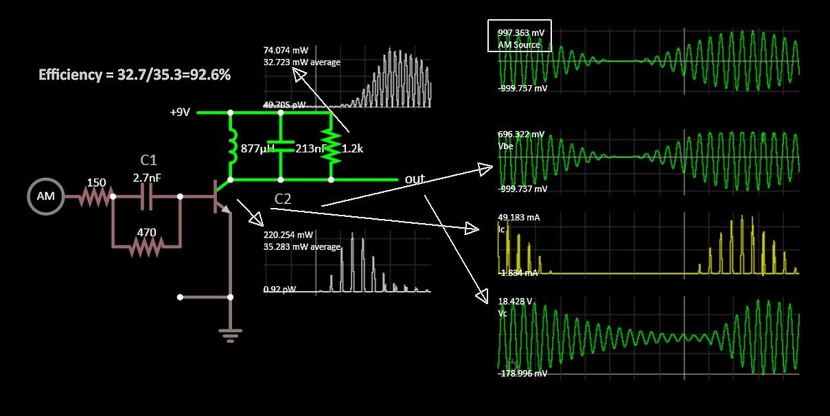
I have simulated this for your here and you can work out your own equations. f(Vin, fmod, Mod index and effic.)

enter image description here

Here I chose 500Hz sine AM on 11.628kHz carrier at 2Vpp.

Since you chose AC coupling, Rbe resister to ground will not work as the cap charges up and doesn't decay.

\$\endgroup\$
9
  • 1
    \$\begingroup\$ Excuse me, but class C amps are heavily non-linear, they cannot amplify properly AM signals. Amplitude modulation in class C amps is done by swinging the operating voltage. \$\endgroup\$
    – user136077
    Commented Jul 1, 2020 at 22:04
  • \$\begingroup\$ Yes you can do that as well perhaps better than how I did it. \$\endgroup\$
    – D.A.S.
    Commented Jul 1, 2020 at 22:20
  • \$\begingroup\$ @user287001 Like this ? tinyurl.com/yb3n6zel \$\endgroup\$
    – D.A.S.
    Commented Jul 1, 2020 at 22:30
  • 2
    \$\begingroup\$ Not quite. 500Hz AC should exist only as summed to the operating DC voltage. The classic AM radio transmitter had usually the secondary of an audio output transformer in series with the DC voltage which was supplied to class C amp. The principle was called in the vacuum tube era "anode modulation". \$\endgroup\$
    – user136077
    Commented Jul 1, 2020 at 22:41
  • \$\begingroup\$ My oversight. I tried but cannot find an efficient bias. tinyurl.com/y9zfbagh \$\endgroup\$
    – D.A.S.
    Commented Jul 1, 2020 at 23:02
0
\$\begingroup\$

Remove R3 and put instead diode 1N4148 . The idea is to allow both signal half cycles have about equal way through a PN junction to prevent C1 collecting any DC. That DC would block the way of the signal to the base of the transistor.

The diode must have opposite direction than the BE junction of the transistor. If your transistor really is PNP as drawn the diode should have its cathode connected to transistor's emitter and anode to the base. If it's NPN as written the diode should be the anode downwards.

Your R3 discharges to some degree the DC which tends to cumulate into C1 but it also loads the signal source and cause losses. I guess that's why you found some optimum R3. If your signal source was as drawn (=no series resistance nor other current limitation) the output of the amp would increase as R3 decreases. Finally it would not be an amp at all because dissipation in R3 would be more than the output.

C1=100uF and no resistance drawn in series with the signal source looks bad. The peak base current could burn the the transistor. Hopefully you have there some resistance in series, say at least 50 Ohm. I guess 1uF capacitor could work well in demonstration purposes and at 11.6kHz its higher reactance gives some protection to the transistor. In addition you can use a ceramic or plastic 1uF capacitor. Electrolytic isn't a good idea without polarizing DC.

You seem to have no load. The LC circuit can develop peak AC voltage = your DC supply if you happen to hit the resonant frequency and there's remarkably low losses in the coil. That AC is summed to the DC when you calculate transistor's peak Vce. Just 9V supply makes total 18V peak to your transistor which isn't fatal but if you have more than 9V beware.

\$\endgroup\$

Your Answer

By clicking “Post Your Answer”, you agree to our terms of service and acknowledge you have read our privacy policy.

Not the answer you're looking for? Browse other questions tagged or ask your own question.