1
\$\begingroup\$

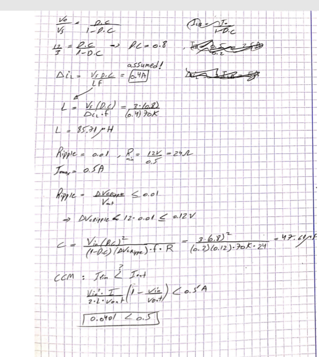
calculations

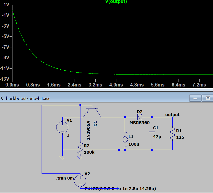
This is my buck/boost converter in the simulation. I get the desired voltage of -12 V but in the real circuit I am only getting -4.88 V, and my transistor heats up; I think it is even burned. I don't know how to turn on and off my transistor safely.

Why am I getting a higher voltage than -12 V?

My transistor is silicon PNP.

the output voltage

\$\endgroup\$
15
  • \$\begingroup\$ "P-channel" is a type of MOSFET, but your circuit uses a (PNP) BJT. Please edit your question to describe your circuit clearly. \$\endgroup\$
    – The Photon
    Commented Jul 6, 2020 at 14:20
  • 4
    \$\begingroup\$ As for why your transistor heats up, you can't just apply -3 V to the base of a BJT. \$\endgroup\$
    – The Photon
    Commented Jul 6, 2020 at 14:22
  • \$\begingroup\$ @ThePhoton why i cant do that? i am applying 3.3V from the raspberrypi \$\endgroup\$ Commented Jul 6, 2020 at 14:24
  • \$\begingroup\$ Because the base emitter junction of a BJT acts like a diode and will draw large currents if you apply more than ~0.7 V (less than -0.7 for PNP) to it. \$\endgroup\$
    – The Photon
    Commented Jul 6, 2020 at 14:27
  • \$\begingroup\$ What a switch circuit I can build to make it work ? I cant change the supply voltage \$\endgroup\$ Commented Jul 6, 2020 at 14:59

1 Answer 1

1
\$\begingroup\$

Following are the answers for the questions asked:

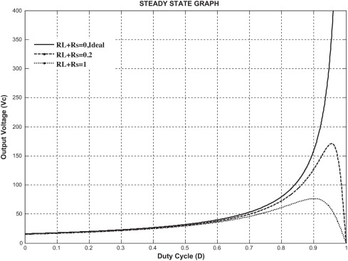
  1. In reality, there are many parasitics involved in circuit which have not been modeled in your Pspice circuit such as inductor comes up with internal resistance(Rl), capacitor has ESR(resistance), source resistance(Rs). Although small but impact on the Voltage ratio is huge. Following graph(from some Paper) shows when you take into account the calculation of these parasitics. Ideal one as provided by you. Usually operating at high duty-ratio is not recommended because of this reason, as it does not follow the formulae correctly. Solution would be to use flyback converter(isolated buck-boost).

enter image description here

  1. Usually when we drive any transistor(that too switch used in power converter), It is recommended not to drive the transistor directly from the micro-controller pins(It is costly). It can damage the pin of your Raspberry Pi. A gate-driver circuit(some idea given below)) should be used for the appropriate transistor.

Comments:

  • MOSFET Driver: Since it acts as capacitive gate. Initial Pulse current would require a small rated transistor between controller and MOSFET
  • BJT Driver: Totem-pole would suffice for that or simple n-p-n transistor also.
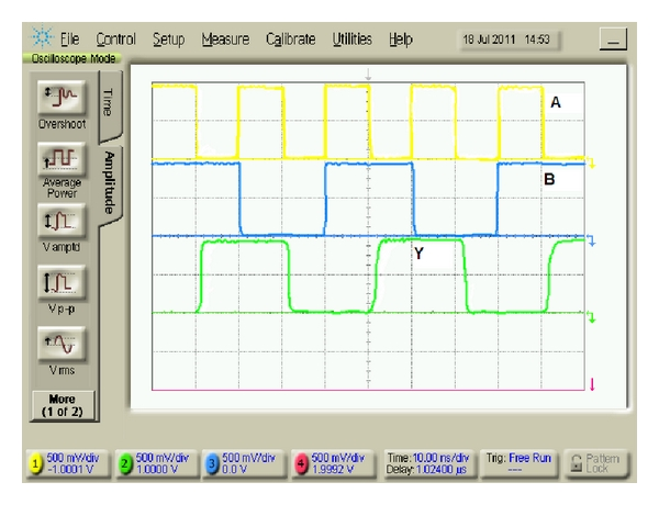
  • While testing, check on oscilloscope the signal of gate/base of transistor. Since the signal would not be proper turn-on and turn off at such high frequency. It would be something like this(Green). (Sometime it has a slant turn-on/turn-off such that duty cycle may go up from 0.8 to 0.95). Voltage will go down further. Kindly take this into account.

enter image description here

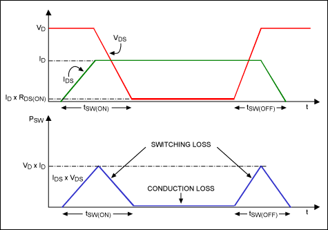
  • The transistor used is 2n2905 which may not be able to support 70k due to high switching losses causing your transistor to heat up.() Stackexchange Link enter image description here
\$\endgroup\$

Your Answer

By clicking “Post Your Answer”, you agree to our terms of service and acknowledge you have read our privacy policy.

Not the answer you're looking for? Browse other questions tagged or ask your own question.