1
\$\begingroup\$

enter image description here

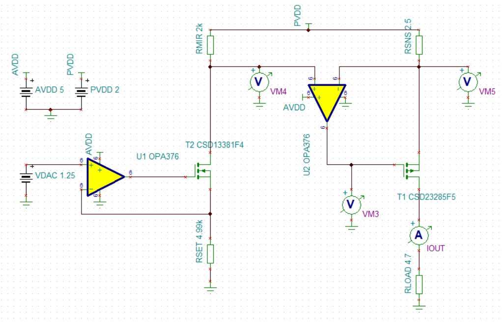
This is a current mirror circuit with 2 op amp stages.

First stage on the left
Voltage from a DAC gets fed into U1 which creates a reference current through Rmir (via the N channel MOSFET) by sensing the voltage across Rset in its feedback loop.

Second stage
U2 (the 2nd stage amplifier) needs to keep the voltage at its two inputs equal as do any op amp. We feed in the voltage across Rsns and the voltage across Rmir to the two inputs respectively.

Non-inverting input
The current across Rmir (reference current) and the resistance of Rmir are constant. Therefore the voltage fed into the non-inverting input is also constant.

Inverting input
The resistance of Rsns is fixed. U2 varies the voltage across Rsns (to match with that across Rmir) by outputting a higher voltage across the MOSFET that then draws more current from PVDD. Hence, across Rsns (and across Rload), we now have a higher current value that is greater than the reference current and that is also constant.

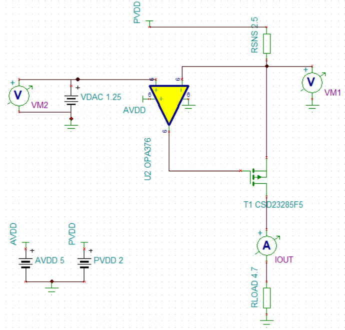
My question is this:
Instead of the constant source that is fed into the non-inverting input of the 2nd stage op-amp, if I feed in the voltage from the DAC directly, why don’t I see a constant current through Rload? I’m aware that the source providing VDAC isn’t a constant current source. But, the current flowing into an op amp is almost negligible right? And it is wholly dependent on the input voltage right?

enter image description here

I know this circuit doesn't work as when I change the Rload to say 2 ohms, the output current changes i.e. doesn't stay constant no matter what Rload's resistance is. Not sure why though.

Also, what would be the feedback loop equation for the 2nd opamp stage with the Mosfet in its way?

\$\endgroup\$

3 Answers 3

1
\$\begingroup\$

Instead of the constant source that is fed into the non-inverting input of the 2nd stage op-amp, if I feed in the voltage from the DAC directly, why don’t I see a constant current through Rload?

It won't work as it stands - to make this work you need to make VM2 (the input demand signal voltage) referenced to the positive supply rail (PVDD) so that the op-amp can manipulate its MOSFET in order to make the voltage at the inverting input PVDD minus VM2. In effect, the first circuit relocated VM2 (with a bit of gain change) up at PVDD.

That's what the original circuit did - if RSET and PMIR were equal values then Vin+ of the op-amp equals PVDD - VM2. The fact that RSET and PMIR are different values is just a signal gain change and not about ensuring that the offsets are correct.

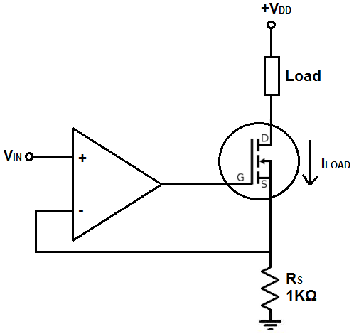
To make this easier to see, consider the constant current sink using an N channel MOSFET: -

enter image description here

The op-amp tries to ensure that the voltage across Rs is the same as Vin.

Turning it upside down and use a P channel MOSFET means that the demand reference point instead of being ground is now the positive rail.

\$\endgroup\$
2
  • \$\begingroup\$ I apologise, I'm not sure I fully understand what you mean by the demand reference point - is it for the first circuit for the first stage, both Vdac and Rset (in the feedback path) is referenced to ground, so no problems there. Whereas, in the 2nd circuit, Vdac is referenced to GND (I get this) and Rsns is referenced to PVDD (?). I assumed any voltage at the inputs of the opamp would always be measured w.r.t. GND. \$\endgroup\$
    – JJT
    Commented Aug 11, 2020 at 18:04
  • \$\begingroup\$ No, that's no how it happens - they are measured with respect to each other and have to be equal in value so, if VM2 is 1 volt then Vin+ has to become 1 volt. That won't happen from what I can see no matter how hard you turn on the MOSFET. \$\endgroup\$
    – Andy aka
    Commented Aug 11, 2020 at 18:23
1
\$\begingroup\$

There are two basic considerations when solving this problem:

The first consideration is to expand the maximum voltage drop across the load aka "compliance voltage of the output current source". It is determined by the supply voltage of the transistor stage minus the voltage drop across the current-setting resistor. If the DAC directly controls the second current source (the OP's idea), this voltage would be only VDAC = 1.25 V while in the original 2-opamp circuit solution it is expanded up to PVDD - VRSNS.

The trick with a current mirror is widely used in the internal op-amp topologies while in the more conventional descrete circuitry it was implemented by cascading n-p-n and p-n-p transistors. BTW, in the case of the OP's configuration, the compliance voltage can be increased simply by amplifying the DAC output voltage so that to approach PVDD but this is a too straightforward solution.

The second consideration is to keep the output current directly proportional to the DAC output voltage. With this purpose, in the 2-opamp solution, they have changed the DAC output reference point from ground to PVDD (as if the DAC output is "turned upside down").

If the DAC directly controlled the second current source (the OP's idea), the output current would be a complementary current. So, to take the right current, you should load a complementary code to the DAC input.

\$\endgroup\$
0
\$\begingroup\$

It can work, however ideally want to have the DAC output ratiometric to the PVDD, and then you will have a voltage at the op-amp non-inverting that varies from some value up to PVDD.

The current at the output will be (PVDD-Vdac)/2.5, which means it works the opposite way of the original circuit (zero output would be maximum current and no compliance).

This means that to get a significant compliance at the output you will need to limit the Vdac to values relatively close to PVDD, but less than PVDD so you will waste some of the DAC resolution.

You have PVDD = 2.0V. The original circuit deliver 0 to 200mA for 0 to 2.5V Vdac, with a maximum current of less than 278mA with a 4.7 ohm load.

If your DAC output varied from PVDD to PVDD - 0.5V (with a maximum above PVDD- 0.695V) you could get similar output current control.

Let's say your DAC actually provides output from 0 to 5V and you can measure the PVDD (which might vary a bit). You could then output the desired voltage, however you would be using only 0.5V of range vs. 1.25V in the original circuit, so a 10 bit DAC would give you less than 6 bits of resolution vs. 8 bits (4:1). Also there would be errors from the voltage measurement which would affect the zero current point.

TLDR: So you lose quite a bit of accuracy and resolution for the simplification, which only removes some inexpensive parts.

\$\endgroup\$

Your Answer

By clicking “Post Your Answer”, you agree to our terms of service and acknowledge you have read our privacy policy.

Not the answer you're looking for? Browse other questions tagged or ask your own question.