5
\$\begingroup\$

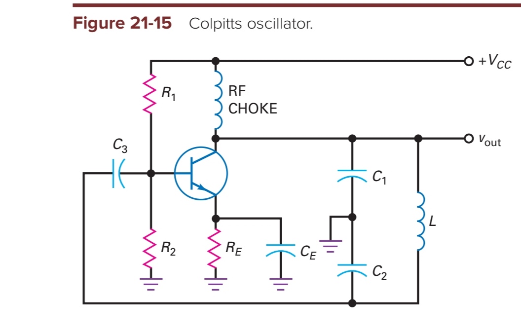
How does the Colpitts oscillator reach the loop gain \$A_V*B\$ of 1?

The loop gain started >>1 (oscillation builds up) but it eventually reaches a state where loop gain is equal to 1(oscillation stabilises). Since feedback is constant \$\frac{C_1}{C_2}\$, it seems to me that \$A_V\$ self-adjusts to the reciprocal of \$B\$. How does that happen?

And why this is only possible to LC oscillators and not to RC oscillators(for example a Wien-Bridge oscillator will not automatically adjust its own loop gain to 1 without using external components like tungsten lamp)

This is the Colpitts oscillator: enter image description here

\$\endgroup\$
7
  • \$\begingroup\$ How does Q amplify signals? And VBE diode dampen them? \$\endgroup\$
    – D.A.S.
    Commented Aug 21, 2020 at 14:39
  • \$\begingroup\$ What is Q? Sorry I don't understand your question \$\endgroup\$
    – hontou_
    Commented Aug 21, 2020 at 14:43
  • \$\begingroup\$ If you understood Q is inverse of damping factor you would \$\endgroup\$
    – D.A.S.
    Commented Aug 21, 2020 at 14:47
  • \$\begingroup\$ So it's the quality factor that lowers \$A_v\$ to reciprocal of B? Isn't Q constant? So at the startup the Q is high but at some time "t" Q lowers so that more energy will be lost and \$A_V\$ to becomes the reciprocal of B? \$\endgroup\$
    – hontou_
    Commented Aug 21, 2020 at 14:51
  • \$\begingroup\$ go read up on Q \$\endgroup\$
    – D.A.S.
    Commented Aug 21, 2020 at 14:52

5 Answers 5

13
\$\begingroup\$

How does the Colpitts oscillator reach the loop gain \$A_V∗B\$ of 1?

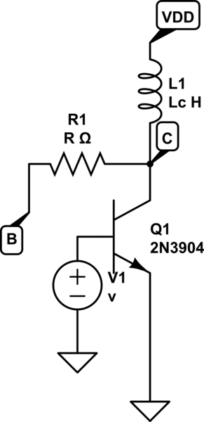
Maybe it's best to use a simulator to show where the gain becomes limited. Here's the “basic” circuit I used and note, that in the first instant, I didn't connect the emitter capacitor C4: -

enter image description here

Note the waveforms; blue is Vout and red is Ve (emitter): -

enter image description here

They "collide" at about 3.1 volts and this prevents any serious increase in output amplitude. In other words, the “basic” common-emitter Colpitts oscillator will always tend to have a significant sinewave distortion.

This Colpitts CE website is now available should more detail be required.

Back to the answer.... It's the same story if I connect C4: -

enter image description here

This time there is a little more output amplitude but again, troughs in Vout collide with Ve and cause asymmetrical clipping. This limits the amplification of the circuit and results in amplitude stability albeit with distortion.

And why this is only possible to LC oscillators and not to RC oscillators for example a Wien-Bridge oscillator

A Wien bridge oscillator will increase its output amplitude until it "crashes" into one of the power rails and therefore attains gain stability through distortion (just as the Colpitts example does).


Some Math

As for the theory behind the frequency of oscillation, you have to regard C1, C2, L and the effective output resistance of the collector acting as a third order network delivering a phase shift of 180 degrees: -

enter image description here

$$\dfrac{V_{OUT}}{V_X} = \dfrac{1}{1+s^2LC_2}\text{ ....take note for later}$$

And, the impedance of C1, L and C2 (\$Z_X\$) is: -

$$Z_X = \dfrac{1+s^2LC_2}{s^3LC_1C_2+s(C_1+C_2)}$$

Therefore (and with a couple of lines of math skipped): -

$$\dfrac{V_X}{V_{IN}} = \dfrac{1 + s^2LC_2}{s^3LC_1C_2R + s^2LC_2 + sR(C_1+C_2) +1}$$

Dividing the transfer functions to get rid of \$V_X\$ yields: -

$$\dfrac{V_{OUT}}{V_{IN}} = \dfrac{1}{s^3LC_1C_2R + s^2LC_2 + sR(C_1+C_2) +1}$$

Noting that for the overall TF to only have a resistive transfer function, the imaginary parts in the denominator cancel to zero hence: -

$$-j\omega^3 LC_1C_2R + j\omega R(C_1+C_2) = 0$$

Therefore R (and of course j) cancel on both sides and, the TF reduces to: -

$$\omega = \sqrt{\dfrac{C_1 +C_2}{LC_1C_2}} = \sqrt{\dfrac{1}{LC_2}+\dfrac{1}{LC_1}}$$

This informs us that the oscillation-frequency feedback is not at the amplitude resonance of L and C2. The oscillation point is on the slope of L and C2 i.e. off amplitude-resonance. You might notice that "R" falls out of the equation and that is also covered a little lower down.

Going back to the main transfer equation (with imaginary parts in denominator at zero) we have: -

$$\dfrac{V_{OUT}}{V_{IN}} = \dfrac{1}{1-\omega^2 LC_2}$$

And, if we plug-in the oscillation frequency (\$\omega\$) we get: -

$$\dfrac{V_{OUT}}{V_{IN}} = \dfrac{1}{1 - \dfrac{C_1+C_2}{LC_1 C_2}\cdot LC_2}$$

And drilling down we find that: -

$$\dfrac{V_{OUT}}{V_{IN}} = -\dfrac{C_1}{C_2}$$

Hence, if C1 equals C2 we get a unity amplitude transfer function for R, L, C1 and C2. If we did a simulation of the third order filter we would see that the value of "R" does not affect the phase angle nor the amplitude response at the oscillation frequency of 2.2508 MHz: -
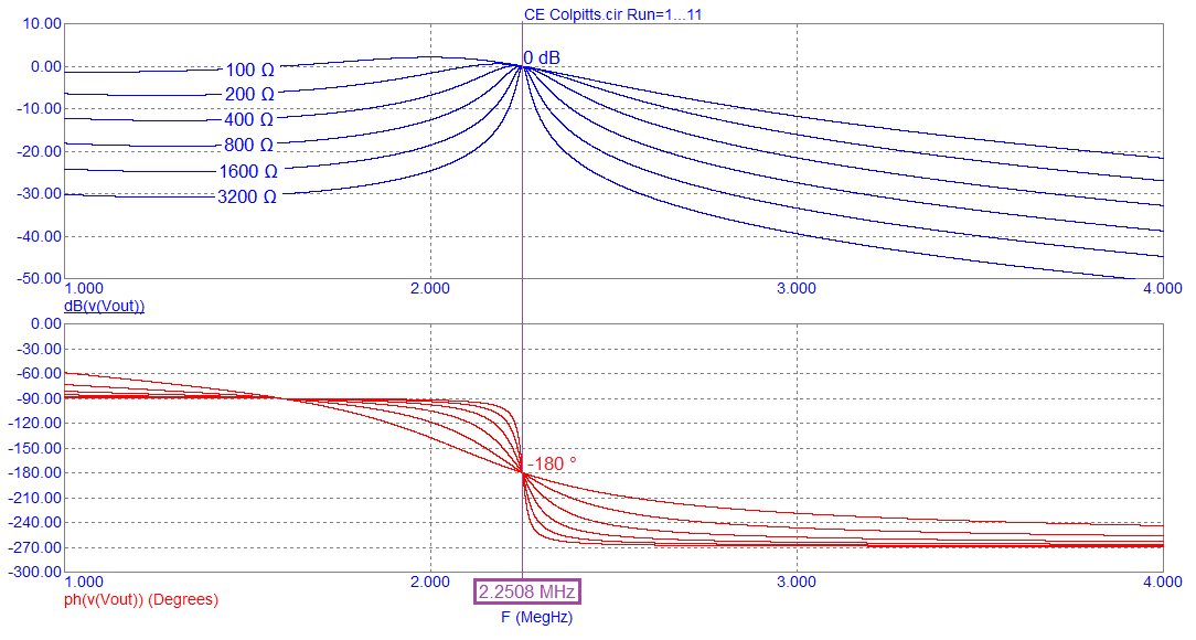
enter image description here

Note that the oscillation frequency is not quite at the amplitude resonance either. It gets pretty indistinguishable at high values of "R" of course.

And, if you did the math, 2.2508 MHz = \$\sqrt{\dfrac{1}{LC_2}+\dfrac{1}{LC_1}}\$


An improvement

Because the common-emitter Colpitts oscillator has plenty of gain it's very likely (in examples on the web) that there will be high distortion levels. I would never consider running one of these circuits with an emitter capacitor because the gain will be too high and asymmetrical clipping will result. In fact, because I have the simulator open, I'd do this to get a decent sinewave: -

enter image description here

Notice the back-to-back diodes (1N4148) that clamp the signal to +/1.4 volts (ish) and notice that the feedback comes via a 33 pF capacitor. I've also reduced the emitter resistor to 470 ohm to allow a tad more headroom and, lowered R3 to 3k3 to lower the bias point: -

enter image description here

That's a 6 volt p-p output and very little sinewave distortion. It's all about providing just enough gain to get the circuit started and having sufficient and progressive gain reduction (as signals rise) to get amplitude stability without too much distortion.

I would probably get rid of the collector inductor and replace it with a 1k8 resistor in many applications: -
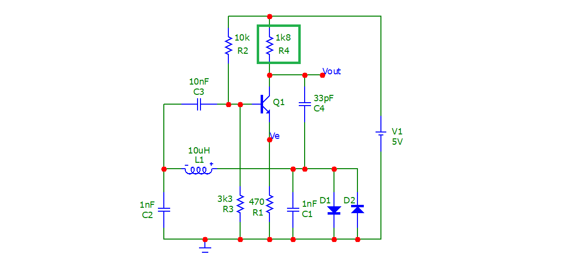
enter image description here

The sine wave amplitude is reduced (as expected) but purity still looks half decent: -
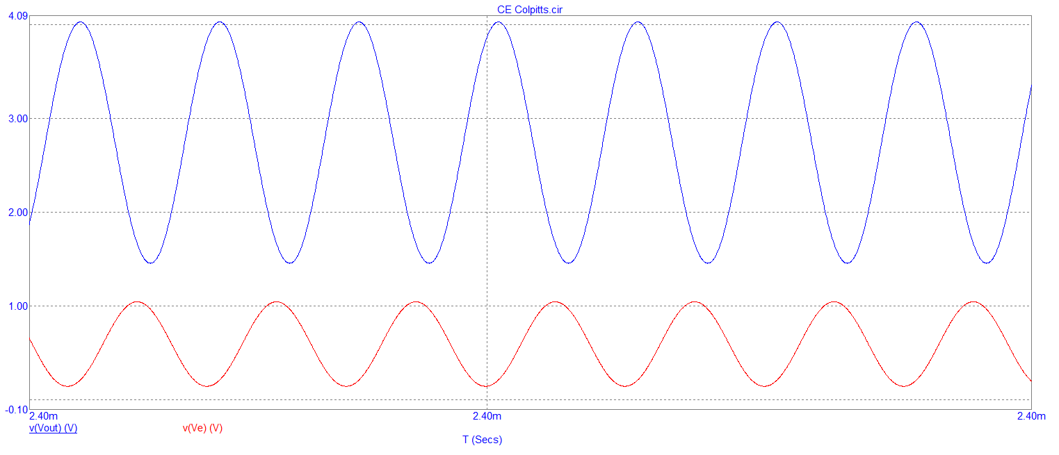
enter image description here

And finally, remember that most circuits on the internet that describe oscillators are very basic in nature and, in most cases, to make a decent practical oscillator requires a little bit of design refinement. After all, if a circuit is described as a sine wave oscillator, you’d probably expect it to produce no visible distortion on an oscilloscope if you bread boarded it.

It’s a shame that many sites don’t go that extra mile.

\$\endgroup\$
12
  • \$\begingroup\$ Now that I noticed it, when using an inductor collector, the sine wave exceeded the source voltage(yours reach 8 volts even if source is just 5 volts). Voltage amplification only happens in series LC circuit right? But in this circuit we use parallel LC tank which is current magnification, I wonder why ? (just curious...) \$\endgroup\$
    – hontou_
    Commented Aug 24, 2020 at 2:01
  • \$\begingroup\$ @IwataniNaofumi the collector inductor has to have an average voltage of zero volts across it else it will be saturated. This means that the average voltage at the collector is the same as the power rail and hence, the AC voltage at the collector must rise equally above and below the supply voltage. It's not a parallel tank; L1 and C2 form a highly resonant low pass filter that can produce significant voltage gain (tens of decibels) around resonance and, if you think about it, L1 and C2 are also in series so, the voltage amplification is the same as a series L and C..... \$\endgroup\$
    – Andy aka
    Commented Aug 24, 2020 at 7:58
  • \$\begingroup\$ There is subtlety here; for instance just look at the image that shows the Vin, Vx and Vout circuit (R, C1, L and C2) just before the derivations of formula. If you plotted that response you would always find that the gain magnitude (Vout/Vin) equals C1/C2 irrespective of R when the phase shift is 180 degrees. If you can't see what I mean I'll add to the answer to show this. \$\endgroup\$
    – Andy aka
    Commented Aug 24, 2020 at 8:02
  • \$\begingroup\$ Ah yes, I simulated the circuit that you had just pointed out and as you have said Vout has a gain of C1/C2 if I make C1 higher than C2. I'm surprised since its a parallel LC tank at one glance but it has the property of a series LC(voltage magnification)! I got it now, thank you for the response \$\endgroup\$
    – hontou_
    Commented Aug 24, 2020 at 8:33
  • \$\begingroup\$ Most websites don't consider that the colpitts is a type of phase shift oscillator that happen to make use of an LC resonant circuit because it rapidly changes output phase over 180 degrees over a small part of the spectrum. That rapid phase change means it has to produce a fairly stable sine wave. It's got nothing really to do with amplitude resonance although that helps loop gain somewhat. But there is the input capacitor and source resistance that give it another 20 degree push so that the actual LC circuit only needs to shift circa 160 degrees to reach the oscillation point. \$\endgroup\$
    – Andy aka
    Commented Aug 24, 2020 at 8:51
3
\$\begingroup\$

The loop gain started >>1 (oscillation builds up) but it eventually reaches a state where loop gain is equal to 1(oscillation stabilises). Since feedback is constant \$\frac{C1}{C2}\$, it seems to me that \$A_V\$ self-adjusts to the reciprocal of B. How does that happen?

As the strength of oscillation increases, the transistor is driven harder and harder into nonlinear operation. This can both reduce the power gain directly, and can start generating harmonics in favor of the fundamental. Eventually the average gain at the fundamental frequency diminishes to \$A_V = \frac{1}{B}\$.

And why this is only possible to LC oscillators and not to RC oscillators(for example a Wien-Bridge oscillator will not automatically adjust its own loop gain to 1 without using external components like tungsten lamp)

It can and does happen with RC oscillators -- it's just that because an RC oscillator doesn't really have a resonator per se., the output would be a pretty crappy sine wave if you (for instance) just let the amplifier limit.

You can make a sorta-good Wien bridge oscillator by designing an amplifying stage that has a time-domain input/output characteristic with a kink in it, so that the average gain goes down at higher amplitudes. If you design the kink so that the loop gain is just barely above 1 for small signals, with a really mild kink, then you can get a stable oscillator with only mild THD -- and then you can spend a bunch of time juggling component values and precisions to get acceptable performance.

\$\endgroup\$
2
  • \$\begingroup\$ I tried simulating the circuit but when I checked the fourier transform or distortion graph , the only harmonic found is the fundamental one. I expected it to produce more harmonics just like what you have said. I wonder why? Maybe it can't detect it? \$\endgroup\$
    – hontou_
    Commented Aug 23, 2020 at 12:07
  • \$\begingroup\$ What were you looking at? In a well-designed Colpitts the voltages should be pretty nice, but the collector and emitter current should be pretty spiky. And -- it's nonlinear, so the devil is in the details. \$\endgroup\$
    – TimWescott
    Commented Aug 23, 2020 at 22:07
3
\$\begingroup\$

There are a few potential mechanisms that reduce Colpitts starting gain back to 1.0 from the starting gain that is greater than 1.0:

  • Voltage limiting (@ collector)
  • re-biasing collector-emitter current (@ base).

Voltage limiting at collector occurs when collector AC voltage grows so large that the base-to-collector junction becomes forward-biased on negative-going peaks. Not a desirable mechanism, because the resonator Q is seriously reduced. But this mechanism controls output amplitude quite well. High-quality, stable, low-noise oscillators avoid this gain-control mechanism.

A desired gain-control mechanism occurs at transistor base. On the positive peak, larger base current flows: on the negative peak, less (or even no) base current flows. This is a weaker gain-control mechanism than collector-base voltage limiting described above. Collector current starts out large enough to start oscillating, then is reduced slightly when oscillating amplitude builds. The voltage waveform at the base of a stable oscillator contains many harmonics. The high-Q LC resonator at the collector acts as a band-pass filter that suppresses high-order harmonics.

A simple Wien-bridge oscillator has little filtering action because the frequency-determining RC elements have very low Q. Furthermore (and more importantly), the gain stage of a simple Wien-bridge op-amp is quite linear - its gain is determined by the ratio of two very linear resistors. So these resistors must establish a loop gain > 1.0 to achieve oscillation. The only gain-limiting mechanism available is voltage-limiting.

\$\endgroup\$
3
  • \$\begingroup\$ "In the positive peak, larger base current flows: on the negative peak, less (or even no) base current flows." - what causes this to happen? \$\endgroup\$
    – hontou_
    Commented Aug 22, 2020 at 0:19
  • \$\begingroup\$ Base-emitter transistor junction is diode-like - it is non-linear. The emitter is biased to a DC voltage, thanks to \$ C_E \$. Base voltage includes a DC voltage, with an AC voltage super-imposed. \$\endgroup\$
    – glen_geek
    Commented Aug 22, 2020 at 0:38
  • 2
    \$\begingroup\$ Andy's answer illustrates transistor voltage limiting at collector nicely, and he gives some suggestions for reducing transistor gain (there are many ways to do this). Ensure that starting loop gain is always > 1.0, but not much more - that's a good trick to achieve. \$\endgroup\$
    – glen_geek
    Commented Aug 23, 2020 at 12:17
3
\$\begingroup\$

Why do you think, that the "feedback" would be C1/C2 ??

The feedback path is a 3rd-order lowpass (ladder structure) which assumes at one single frequency (the desired oscillation frequency) a phase shift of -180deg. The other 180deg are caused by the inverting function of the BJT. Hence, the phase portion of the oscillatiuon condition can be fulfilled.

If the loop gain at t=0 (oscillation start) is larger than unity, the amplitudes are growing until the physical limit (supply rail) is reached. This lowers the gain and fulfills the amplitude portion of the oscillation condition.

When the loop gain at t=0 is only slightly above unity the non-linearity of the transistors parameter may limit the gain for rising amplitudes (before clipping occurs).

Alternative explanation (based on a tank circuit):

For another explanation of the feedback circuit we can start with a parallel combination (tank circuit) L||C with C=C1C2/(C1+C2). Without grounding the common node between C1 and C2 there is one single frequency (resonant frequency) where there is no phase shift between the voltages at both ends of the tank circuit against ground.

Now, if we ground the node between both capacitors the whole circuit will keep its frequency dependent properties (resonance without phase shift caused by parts properties) - however, we force both ends of the tank circuit now to have different signs (phase inversion, 180deg phase shift). This is the only physical alternative to have a voltage across the series connection of both capacitors when the midpoint is grounded. Of course, due to different capacitances, both voltages at these points (against ground) are different (very often factor 10 or so...)

The resistive parts on both sides of the tank (output resistance at the collector, input resistance at the base) can be seen approximately as damping resistors for the idealized tank.

EDIT: Feedback factor

When Ro is the finite output resistance at the collector node, the transfer function between input (node A) and output of the frequency-dependent feedback network (3rd-order lowpasss, without the resistive load at the base) is:

G(s)=1/[1+s(C1+C2) + s² * L * C2 + s^3 * Ro * L * C1 * C2].

At the oscillation frequency the function is real and negative - hence, the imag. part is zero. Setting the imag. part of G(s) equal to zero gives the well known expression: wo=SQRT[(C1+C2)/C1C2*L].

If we introduce this frequency into the real part of G(s), we arrive at

G(jw=jwo)=1/[1-(C1+C2)/C1]=-C1/C2.

\$\endgroup\$
7
  • \$\begingroup\$ The typical explanation of a Colpitts oscillator in amateur radio literature shows a common-collector Colpitts, and describes the feedback as being C1/C2. And, for a high-Q tank circuit and low loading from the transistor, at the frequency of operation, \$v_{be}\$ is, indeed, pretty close to the ratio C1/C2 times the coil voltage. \$\endgroup\$
    – TimWescott
    Commented Aug 21, 2020 at 15:49
  • \$\begingroup\$ @TimWescott a common-collector colpitts oscillator has gain due to the L and two Cs of \$\frac{C1+C2}{C2}\$. Maybe you can link an article? \$\endgroup\$
    – Andy aka
    Commented Aug 21, 2020 at 17:55
  • \$\begingroup\$ @Andyaka, you're right. The caffeine hadn't kicked in when I made that response. By and large, though, there's a feedback that is determined by that voltage divider. I have no article to link to, but grab any ARRL Handbook from about 1975 to the present and you'll find it described that way. \$\endgroup\$
    – TimWescott
    Commented Aug 21, 2020 at 18:15
  • 1
    \$\begingroup\$ @Tim CC colpitts gain proof in my answer. \$\endgroup\$
    – Andy aka
    Commented Aug 21, 2020 at 18:25
  • 1
    \$\begingroup\$ Tim - I think, we do not need any handbook or link - we just have to look on the circuit and see the 3rd-order lowpass circuit, don`t you? \$\endgroup\$
    – LvW
    Commented Aug 22, 2020 at 7:52
2
\$\begingroup\$

Before answering your question, let me explain briefly how this Colpitts topology works. Then, I will answer your main question.
Working of the Colpitts Oscillator
Consider an LC tank with node between the capacitors grounded as shown below:

schematic

simulate this circuit – Schematic created using CircuitLab

You might know from basic electronics that if the capacitors have some initial charge, then the LC tank will start oscillating. Let \$v_A\$ be the voltage at node A and \$i\$ be the current through the capacitors then, voltage at node B, \$v_B\$, will be: $$v_B = i.\frac{1}{sC} = -v_A$$ Thus, the LC tank will have opposite voltages at its two ends A and B. In other words, between A and B LC tank has a transfer function \$-1\$. Due to the losses inside the tank the oscillations would eventually die out unless there is some positive feedback.
Now consider putting this tank across an inverting amplifier as shown below:

schematic

simulate this circuit

Since there are two inversions in the loop as shown by the arrows, a positive feedback is created which compensates for the tank losses and results in sustained oscillations.

Oscillation Start-up

For oscillation amplitude to build up, it needs to be ensured that the positive feedback has sufficient loop gain. Let's calculate it.
You might know that a real LC tank is modelled as a parallel combination of L, C and resistor R which models the tank losses. At resonance, the LC part has infinite impedance so the tank can be represented by just its resistance R. In this situation we have a circuit as shown:

schematic

simulate this circuit

Here I have broken the loop at node B to calculate the Loop gain. It can be easily calculated to be: $$L = g_mR$$ For oscillation buildup, \$L\gt 1\$, thus \$g_m \gt \frac{1}{R}\$.

Amplitude feedback during Steady State Oscillation

Suppose we have a system with clipping non-linearity as shown:

enter image description here

Suppose we give it a sinusoidal input with amplitude A and frequency f. As long as, the gain is less than the range of the clipping non-linearity (NL), the input comes out undistorted. For gain greater than the range of the NL, output will be clipped and the amplitude of the fundamental component will be given by: $$A_o = \frac{4A_c}{\pi}$$ The gain of the system at this frequency becomes: $$G = \frac{A_o}{A} = \frac{4A_c}{\pi A}$$

Thus the gain of the system falls at higher amplitudes.
The transconductance of transistor actually behave quite similar to such non-linear system. Due to supply or current limitations and device non-linearity, the \$g_m\$ does not stay constant for all amplitudes instead starts to fall for larger amplitudes. For instance, in your case, the maximum current corresponds to \$I_{max} = \frac{V_{DD} - V_{CEsat}}{\omega L}\$. Above this current, the transistor ceases to be in active region. The \$g_m\$ can be plotted against amplitude and is shown below: enter image description here

It is easy to see the amplitude feedback now.
For amplitude smaller than \$A_{osc}\$, \$g_m \gt \frac{1}{R}\$ resulting in high loop gain and increasing amplitude.
Similarly, for amplitude smaller than \$A_{osc}\$, \$g_m \lt \frac{1}{R}\$ resulting in low loop gain and decreasing amplitude.
Due to this feedback created by the non-linearity of the circuit, the amplitude remains stable at \$A_{osc}\$, where loop gain is 1.

Hope it answers your question.

\$\endgroup\$
1
  • \$\begingroup\$ All comments have been moved to chat here. There was some good technical exchange there BUT several people were getting less polite with each other than is useful. All concerned: Please attempt to maintain professional demeanor even if you consider the other party is, perhaps, an idiot. \$\endgroup\$
    – Russell McMahon
    Commented Aug 22, 2020 at 11:12

Your Answer

By clicking “Post Your Answer”, you agree to our terms of service and acknowledge you have read our privacy policy.

Not the answer you're looking for? Browse other questions tagged or ask your own question.