1
\$\begingroup\$

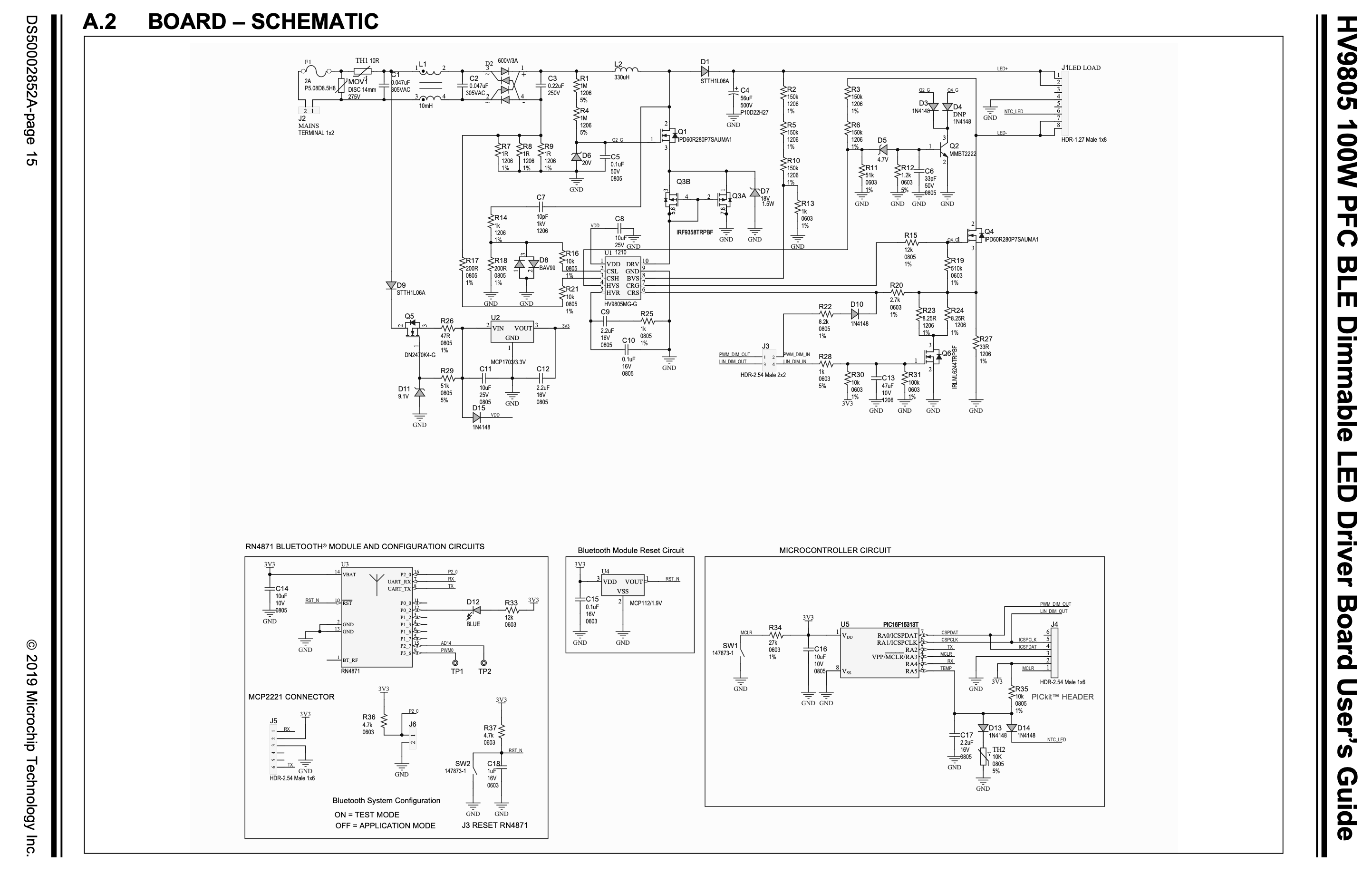
Attached is a schematics page from Microchip's development board. This question is only about the 3V3 power supply they use for powering their PIC circuit.

Can someone minimize this schematic to the bare 3V3 power supply? Maybe mark the necessary components with color or list them in a text. I would like to be able to build just the 3V3 power supply without the rest of the circuit, to power a simple PIC circuit with blinking LED. Mind you, I have other solution working, I just wanted to really understand the Microchip's solution, which looks simpler then mine.

I want to learn from this, how this supply works. Specifically, I do not clearly see how the LDO ground gets returned back to 230VAC main. How does the Q5 FET even opens (where the gate voltage comes from)?

Thank you for taking time to explain this. I am sure I am missing some crucial detail here.

enter image description here

\$\endgroup\$

2 Answers 2

5
\$\begingroup\$

Q5 is a depletion mode FET. It is normally ON unless turned OFF with the gate voltage.

The LDO ground path that returns to mains happens via R7 - R9 as that equals to only 0.33 ohms total resistance.

\$\endgroup\$
2
  • 1
    \$\begingroup\$ +1 for noticing Q5 is depletion mode \$\endgroup\$ Commented Sep 15, 2020 at 9:38
  • 1
    \$\begingroup\$ @Justme: Right there, it was worth to ask the question - I learned about depletion FET. That was bugging me, how the gate opens - and it was opened already! Bimpelrekkie answered a lot also, so I have a dilemma on accepting and answer and it can be only one - but I think your answer took care of the crucial one. \$\endgroup\$ Commented Sep 16, 2020 at 17:53
6
\$\begingroup\$

This application board does not appear to be using an isolated supply. That means that any point in the circuit can carry mains live voltage and must therefore be in an isolated (plastic) box. This design is really only for engineers that have experience with mains-live circuits.

The circuit to derive the 3.3 V consists of a pre-regulator (MOSFET Q5 and zenerdiode D11) and a standard 3.3 V voltage regulator chip. MOSFET Q5 takes care of most of the voltage drop. This can be done if the current that is needed is small (a couple of mA).

The ground of this circuit is a "local ground" meaning it is not connected to mains ground or even to anything else. As I said: this board needs to be inside its own isolated box!

The ground is "made" at the - pole of C3 (just after the bridge rectifier). The mains voltage is rectified and the resulting (high) DC voltage appears across C3. The - pole of C3 is connected (through R7, R8, R9 = 0.33 ohm) to a node that is defined as being "ground". The circuit makes its own ground! Note that ground is just a reference point and as such you're free to choose whatever point you like (some points make more sense to select as ground than others).

My advise to you is to ignore this circuit (at least for building your own stuff, for education it is OK) and use a much simpler and safer solution:

  • use a USB power adapter, like one that is used to charge a phone. Use a USB cable to get a safe 5 V from that.

  • then use a 3.3 V regulator module to lower that 5 V into a stable 3.3 V. You can buy such a 3.3 V regulator module at many places. On such a module there will be a voltage regulator chip similar to U2 on the dev. board you show.

\$\endgroup\$
1
  • 1
    \$\begingroup\$ Thank you for a lot of details. I had a dilemma with the other much shorter answer, but a crucial explanation. Sorry I cannot accept two answers :( but the least I can do is +1 to you \$\endgroup\$ Commented Sep 16, 2020 at 17:54

Your Answer

By clicking “Post Your Answer”, you agree to our terms of service and acknowledge you have read our privacy policy.

Not the answer you're looking for? Browse other questions tagged or ask your own question.