1
\$\begingroup\$

this is my first attempt ever at building an H bridge for brushed DC motors. The board is controlled externally with an Arduino that sends the EN and PWM signals. I also need to measure the motor current to do torque/current control. For current sensing I decided to adopt low-side sensing with shunt resistor (10mOhm) and op-amp in non-inverting configuration to amplify the voltage drop.

The bridge-part of the board works quite as expected, I'm able to move a dc motor in both directions with varying duty cycle, but I have 2 problems:

  1. Not crucial, but I noticed that the Green LED (I put it in order to signal that the board is powered) turns on even when the VBATT is disconnected if I apply the EN signal from the Arduino, and I really can't understand why.

  2. Current sensing is not working. When I just power the circuit with a DC power supply I have 0.08A drawn by the op-amp. If I remove the IC, the current goes to 0. If I apply PWM, at 0.27A drawn from the supply (of which 0.19A = 0.27A-0.08A are due to the motor) I have:

  • 1.9mV across the shunt resistor (which is reasonable, at 0.19A * 10mOhm)
  • 1.9mV on the opamp non inverting input (of course)
  • 0.42V on the opamp inverting input (?). This value is more or less fixed varying duty cycle.
  • 10.63V on opamp out (?). This value is more or less fixed varying duty cycle.

Moreover, the op-amp gets rather hot in few seconds. I already double checked the pcb for shorts or wrong connections. To measure I'm using a multimeter since at the moment I don't have an oscilloscope at hand, planning on buying one.

So the questions are:

  1. Why is the green LED turning ON when it is not supposed to
  2. Why is the op-amp amplifier not working as expected
  3. If possible, some recommendations on better ways/components for current sensing.

PS. At the moment I considered only through hole components for ease of soldering, but for future versions I will probably consider also SMD components.

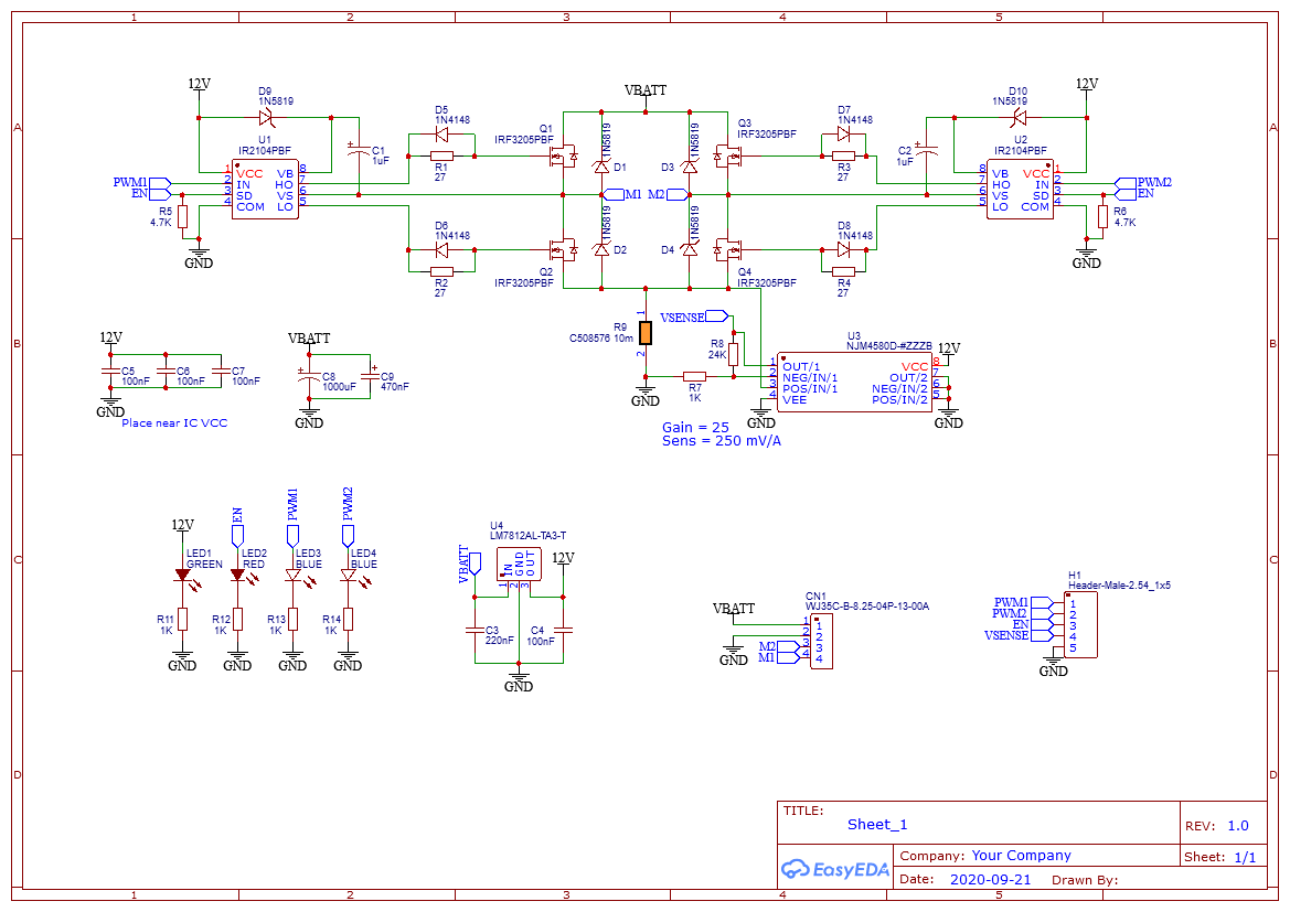
Brushed DC motor H Bridge schematic

\$\endgroup\$
2
  • 1
    \$\begingroup\$ Are you sure it's a good idea to ground the unused Output of the 2nd half of your opamp? \$\endgroup\$
    – brhans
    Commented Oct 7, 2020 at 19:47
  • \$\begingroup\$ To be honest, no. I did it without thinking too much. In next designs I would use the other OA as a voltage follower, or change OA altogether using a single channel CMOS rail-to-rail OA as suggested in other answer (something like TLV271) \$\endgroup\$ Commented Oct 10, 2020 at 10:58

1 Answer 1

2
\$\begingroup\$
Why is the green LED turning ON when it is not supposed to

Failure to recognize ESD input clamp to Vdd is powering up the 12V rail with logic input voltage. ( bad idea and cause for latch-up fault possible)

Why is the op-amp amplifier not working as expected

Failure to read datasheets V common mode input range is +/-12 for +/15V supply (meaning required input must exceed bottom rail by 3V for biasing.

If possible, some recommendations on better ways/components for current sensing.
  • Use equal balanced resistors to shift both inputs near V/2 and achieve same gain.
  • choose Rsense for approx 50mV full scale for worst case locked rotor current. due to power dissipation. Usually choose Pd of R at 50% of rated value for ~70'C rise. -Consider braking current (BEMF) is negative , consider Vout=idle at Vref/2 to measure bipolar currents, if you want otherwise not
  • Consider CMOS OA for Rail to Rail input and output but observe ESD precautions and latchup protection of moving motor and power off then ON
\$\endgroup\$
2
  • \$\begingroup\$ Thanks for the reply and the recommendations. Now I think I fully understand the op-amp common mode issue and how I could possibly solve it maintaining this design. However I do not understand the ESD issue, who is powering the 12V rail, why it happens only when EN is active, how could I properly change the design to "observe ESD precautions and latchup protection". \$\endgroup\$ Commented Oct 10, 2020 at 10:53
  • \$\begingroup\$ stray inductive noise from motor wires can be reduced using twisted pairs. Your schematic cannot show all the wire inductive or crosstalk without a photo of layout 10nH/cm. This can create more voltage than the resistor depending on layout. thus raising the differential input RK’s on both sides with int/ext clamp Sch diodes to rails will prevent overshoot \$\endgroup\$
    – D.A.S.
    Commented Oct 10, 2020 at 16:48

Your Answer

By clicking “Post Your Answer”, you agree to our terms of service and acknowledge you have read our privacy policy.

Not the answer you're looking for? Browse other questions tagged or ask your own question.