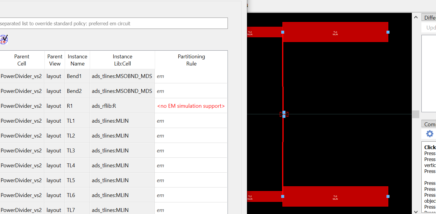
Unless you have EM model of resistor you cannot simulate it. Change the partition rule to circuit and run meshing and EM simulation. After that, create a component of this layout and place this as component this in a new schematic. The component looks like layout with pins at port ends and resistor. Now add the resistor in schematic and simulate S- Parameters.
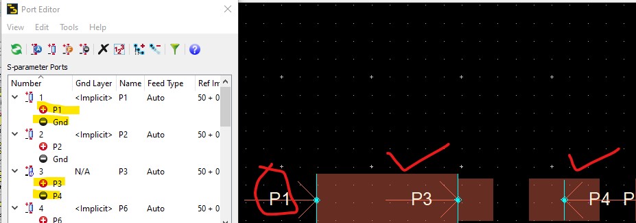
Don't forget to place pins at the location you are placing resistor. They shouldn't be wrt to GND!
Check out this example image I have cropped out from one of my design

Pins 1 is wrt gnd which acts as Port 1 where as I place a passive component between port 3 and 4.
Check out this link for procedure to converting layout to component and simulating it.
This is example of microstrip filter.


