1
\$\begingroup\$

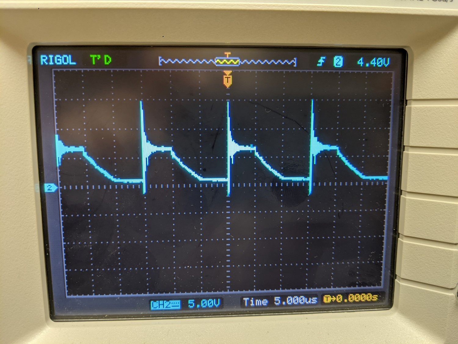
I recently set up a circuit with an ADA4870 op-amp for driving an ultrasonic Piezo element. I chose this specific op-amp because it was advertised as having a slew rate of up to 2500 V/us (symmetric on rise and fall) on a 10-40V power supply. To test it I set it up with +30V for positive power, GND for negative power, and two 2.4k resistors from out to V- and V- to GND (for a 2x gain with feedback). I then fed in an Arduino digital signal set to be high for 5us and then low for 10us. The measured input waveform is a sharp step function, but the output from the op-amp looks like this:

scope output

The rise is very sharp as expected, but the fall is extremely slow at roughly 1 V/us. Normally a slow rise/fall time would make me suspect parasitic capacitance somewhere, but I can't see why that would slow down the fall time but not the rise. Does anybody have an idea of why this might be showing up?

\$\endgroup\$
3
  • 2
    \$\begingroup\$ The characteristic graphs in the datasheet all appear to be generated using dual supplies and an input voltage referenced to ground in the center. The Input common-mode voltage spec is also +/-18V with a dual +/-20V supply (so telling you to stay at least 2V away from each rail). I suspect that it doesn't like the 0V input you're giving it with that single 30V supply. \$\endgroup\$
    – brhans
    Commented Nov 17, 2020 at 0:59
  • \$\begingroup\$ Hello, Dominic, I can’t answer your question, but can make some suggestions. Set up the circuit like figure 69 in the data sheet. You should get very similar response to the data sheet graphs, then. Because this is a current feedback op amp, you cannot arbitrarily choose the feedback resistor. For circuits like this, you need to keep all the wires super short. Take special care with the ground point. All wires to there must be short and direct. \$\endgroup\$
    – user69795
    Commented Nov 17, 2020 at 1:04
  • 2
    \$\begingroup\$ Show your schematic. Include power rail voltages and load. \$\endgroup\$
    – Andy aka
    Commented Nov 17, 2020 at 9:02

2 Answers 2

1
\$\begingroup\$

Basically using a single supply, you must ensure the input stays in the Vcm spec range which is >2V or <Vcc-2V. otherwise the input is not operating in close loop linear range. (E.g. Vcc/2 is a good way to bias inputs if possible by AC coupling.)

Other fine details,

Ringing is most likely from excessive probe ground lead and for <=35ns Tr or >=20 MHz you disable the DSO video filter and reduce ground leads to 1cm or so with special probing methods. (Repeated often on this site)

To minimize stray C load current , minimize differential ground capacitance and match impedance from cable to load which is the root L/C ratio.

\$\endgroup\$
1
  • \$\begingroup\$ The problem was that I was using 0 and +30V rather than +/-15V; it really didn't like in the input going down to the negative rail \$\endgroup\$ Commented Nov 18, 2020 at 1:20
1
\$\begingroup\$

Suggestions

  • build the circuit atop a single_sided copper_clad FR-4, so you have a Ground Plane to work with

  • bypass the VDD using 0.1uF from VDD to Ground using 0.1 inch lead. Locate this capacitor at the OPAMP VDD pin.

  • isolate your opamp VDD from the power supply, by inserting 10 ohms in series. This dampened any wire_ringing.

  • phase shifts on the Vin- may cause ringing or oscillation; consider using 1Kohm or 470 ohm resistors, instead of 2.4K

  • Bias your Vin+ to VDD/2 using 1Kohm and 1Kohm voltage divider.

  • inject the MCU rectangular wave using 0.1 uF to VIN+; the TAU of 0.1uF and 500 ohms is 50 microseconds, so you may see some droop on the waveform

\$\endgroup\$

Your Answer

By clicking “Post Your Answer”, you agree to our terms of service and acknowledge you have read our privacy policy.

Not the answer you're looking for? Browse other questions tagged or ask your own question.