-1
\$\begingroup\$

I'm really struggling with a VHDL implementation of a debouncing circuit for 2-position slider switches.I had initially planned to use an SR latch to do this but couldn't figure out how to make it work. (I'm using a Basys 3 board with Artix-7 FPGA).

I believe the problem is the way that the switches are connected to the FPGA. I found this video to be very helpful in explaining the SR latch, but he has an active low SPDT switch with two outputs. My switches appear to be connected the opposite way round, as shown in the image below which is from the Basys 3 datasheet.

enter image description here

One switch position is powered, and the other is grounded. Then there's a single output to the FPGA. Firstly, if this kind of switch has a particular name, can someone tell me what that is? I assumed these were SPDT switches but this configuration makes me think they're not, and I also don't know what the arrows on the switches indicate? Does it mean that the default position is grounded?

Either way, since the switch doesn't have 2 outputs to the FPGA, using an SR latch doesn't seem viable as it requires two inputs - one for each NAND gate.

Can anyone provide some info on these switches so I can research some more, since I don't seem to be able to find any info about this configuration, and the datasheet doesn't provide any info except this image. And if possible, can you suggest a method to debounce a switch like this, either in VHDL or hardware(a circuit at the switch output, not a change to the existing hardware)?

Edit: one method I've tried is using a counter which allows 10ms for the input to settle. If the input changes due to switch bounce, it will restart this counter. This works, but it means that there's a delay which I'm worried will cause timing issues. As you can see in the simulation below (which has simulated bounces for 10ms), the debounced output is unbounded until about 20ms, because it has counted 10ms after the final rising edge of the bounces. I'd prefer a method which works more like the SR latch, where it latches the input straight away. Is this possible? enter image description here

\$\endgroup\$
12
  • \$\begingroup\$ you could still use the SR method in the video ... two switches would be used as one input ... only one would be connected to GND at any time ... cumbersome, but doable ... additional logic could be implemented to ignore both switches being low \$\endgroup\$
    – jsotola
    Commented Nov 30, 2020 at 18:32
  • \$\begingroup\$ @jsotola thats a good idea actually but not really viable for my application as I need to use specific switches. I'll keep it in mind in case I can't find anything better though, thanks \$\endgroup\$
    – MendelumS
    Commented Nov 30, 2020 at 18:35
  • 2
    \$\begingroup\$ this is not really related to the question that you asked ... are you absolutely certain that the slide switches actually need to be debounced? ... how are you using the switches in your application? \$\endgroup\$
    – jsotola
    Commented Nov 30, 2020 at 18:41
  • \$\begingroup\$ Yes they are being used to control a data generator. The combination of switches used determines what mode the data generator is set to. Since the system uses a 100MHz clock, any bouncing inputs could cause false triggers that generate incorrect data. For example lets say a '01' input combination from two switches generates '0001', and a '00' combo generates '1110'. When the switch is flicked it would bounce and so the input would change between '00' and '01', outputting both data sets instead of just the one that is intended. \$\endgroup\$
    – MendelumS
    Commented Nov 30, 2020 at 18:49
  • \$\begingroup\$ pictures of the Basys 3 board on the internet show that the switches are open on ends ... it may be possible to insert thin strip of mylar to break the connection between the slider and GND and slip in thin wire to connect to the slider, and therefore to the data pin ... then you could add external switches wired for the SR configuration \$\endgroup\$
    – jsotola
    Commented Nov 30, 2020 at 18:58

3 Answers 3

0
\$\begingroup\$

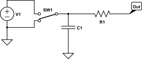
I don't know the details of your application, but adding a capacitor to ground between the spdt switch and the resistor will quelch contact bounce. If the switch bounces while connecting or disconnecting to the high rail, the capacitor will hold a charge during that bounce, and similarly when the switch is connecting or disconnecting to ground. The capacitance required depends upon how much current your circuit draws from the switch, and how long it is possible for the switch to bounce.

schematic

simulate this circuit – Schematic created using CircuitLab

\$\endgroup\$
5
  • 1
    \$\begingroup\$ Thanks but this wont work as I can't make any changes to physical hardware. Its a prebuilt FPGA board so all the hardware is already there. I'm looking for a way that I can debounce the signal as it enters the FPGA. \$\endgroup\$
    – MendelumS
    Commented Nov 30, 2020 at 18:16
  • \$\begingroup\$ Can you modify this line from your question then? "And if possible, can you suggest a method to debounce a switch like this, either in VHDL or hardware?" \$\endgroup\$ Commented Nov 30, 2020 at 18:26
  • 1
    \$\begingroup\$ Ah yes I can see how that was misleading - I just meant a hardware circuit that I can recreate in VHDL. Not changes to the existing hardware. \$\endgroup\$
    – MendelumS
    Commented Nov 30, 2020 at 18:29
  • \$\begingroup\$ @MathKeepsMeBusy Shouldn't R1 be placed between SW1 and C1 to form a simple RC filter? \$\endgroup\$
    – Velvet
    Commented Feb 2, 2022 at 21:15
  • 2
    \$\begingroup\$ @Seir It can be done that way. However, a resistor between the switch and capacitor will cause a delay in the output. With no resistor there, when the slide switch breaks one connection, the capacitor will hold the last value for a short time. Then, as soon as the slide switch makes contact in the new position, the capacitor and output will change state. \$\endgroup\$ Commented Feb 3, 2022 at 1:55
0
\$\begingroup\$

You really have two issues to deal with here. First, you need to deal with metastability. To do that, you'd typically connect up an inverter to one of the inputs of your SR flip flop (creating a D flip flop), so you can drive both the inputs to your SR from your single switch:

schematic

simulate this circuit – Schematic created using CircuitLab

Then you normally want to run that signal through another flip flop to synchronize it with the clock on the rest of your system.

schematic

simulate this circuit

Just to be clear, both of those will be clocked with your system clock.

After that, you do your debouncing. Typically, you do this with a counter that starts running when you see (say) a high signal, and resets when you see a low signal. Then you produce an output when (and only when) the counter reaches some upper limit (long enough to cover bouncing).

I've never actually tried to implement it, but I think you could probably sort of reverse the order of those things if you wanted. Instead of sampling and then counting down to cover switch bounces, you could probably do a count on your clock to produce a clock for the flip flops with a very low duty cycle. For example, if you're using a 10 MHz clock for the rest of the system, feed the flip flops with a clock that has one high pulse every 50 ms, so it samples the signal from the switch for .1 uS every 50 ms.

It seems like this could have at least some advantage with an FPGA, by allowing you to do more of the work with dedicated clock management resources, and reserve the fabric for your other logic.

But as I said, I've never actually tried that, so I wouldn't call this a recommendation, just a thought you might find interesting.

\$\endgroup\$
0
\$\begingroup\$

From reading through the comments, I think that you need to rephrase your question to "What's the best way to debounce multiple slider switches?" especially pertaining to the comments by Chris Stratton about intermediate values.

Intermediate values will be generated when changing two or more sliders at the same time, i.e. to the human brain it appears to be almost simultaneous, but to your FPGA running at 100 MHz, many clock cycles will occur between the slider changes.

For that you will need a bus debouncer that treats the multiple switch positions as a single value where any change on any slider will reset the common debouncer counter.

Bus Debouncer

This debouncer assumes its inputs are synchronised to the clock.

library ieee;
use ieee.std_logic_1164.all;
use ieee.numeric_std.all;

entity Debounce is
    generic
    (
        CLOCK_PERIOD   : time := 10 ns;
        DEBOUNCE_PERIOD: time := 100 ms;  -- Rule of thumb for a slider switch.
        BUS_WIDTH      : positive := 16
    );
    port
    (
        clock : in std_logic;
        input : in std_logic_vector(BUS_WIDTH - 1 downto 0);                      -- Synchronous but noisy input.
        output: out std_logic_vector(BUS_WIDTH - 1 downto 0) := (others => '0');  -- Debounced and filtered output.
        change: out std_logic := '0'                                              -- Goes high for 1 clock cycle when debounced.
    );
end entity;

architecture V1 of Debounce is

    constant MAX_COUNT: natural := DEBOUNCE_PERIOD / CLOCK_PERIOD - 1;
    signal counter: natural range 0 to MAX_COUNT := 0;  -- Specify the range to reduce number of bits that are synthesised.

begin

    process(all)
        variable v_change: boolean := false;
    begin
        if rising_edge(clock) then
            counter <= 0;   -- Freeze the counter by default to reduce switching losses when input equals output.
            change <= '0';

            if counter >= MAX_COUNT then    -- If successfully debounced, notify what happened.
                output <= input;
                change <= '1';
            elsif v_change then             -- Hysteresis.
                counter <= counter + 1;         -- Only increment when input and output differ.
            end if;
        end if;

        -- Change detection compares the input bus with the output bus and flags any discrepancy.
        v_change := input /= output;
    end process;

end architecture;

Synchroniser

You also need a bus sychroniser to synchronise all the slider switch inputs to the clock before feeding them to the debouncer.

library ieee;
use ieee.std_logic_1164.all;
use ieee.numeric_std.all;

entity Sync is
    generic
    (
        SYNC_BITS: positive := 3;  -- Number of bits in the synchronisation buffer (2 minimum).
        BUS_WIDTH: positive := 16
    );
    port
    (
        clock : in std_logic;
        input : in std_logic_vector(BUS_WIDTH - 1 downto 0);  -- Asynchronous input.
        output: out std_logic_vector(BUS_WIDTH - 1 downto 0)  -- Synchronous output.
    );
end entity;

architecture V1 of Sync is

    constant SYNC_BUFFER_MSB: positive := SYNC_BITS - 1;
    subtype TSyncBuffer is std_logic_vector(SYNC_BUFFER_MSB downto 0);
    type TSyncBuffers is array(0 to BUS_WIDTH - 1) of TSyncBuffer;
    signal sync_buffers: TSyncBuffers;

begin

    assert SYNC_BITS >= 2 report "Need a minimum of 2 bits in the synchronisation buffer.";

    process(all)
    begin
        if rising_edge(clock) then
            for i in 0 to BUS_WIDTH - 1 loop
                sync_buffers(i) <= sync_buffers(i)(SYNC_BUFFER_MSB - 1 downto 0) & input(i);
            end loop;
        end if;
        for i in 0 to BUS_WIDTH - 1 loop
            output(i) <= sync_buffers(i)(SYNC_BUFFER_MSB);
        end loop;
    end process;

end architecture;
\$\endgroup\$
3
  • 1
    \$\begingroup\$ Thank you for also recognizing this as the critical issue. However, I'm not sure that you can de-bounce the combined value, as this assumes that the human is only going to stop changing things when the combination is fully correct - in effect, you'd need a long debounce delay of several seconds. I really think the simplest solution would be basically to have a "commit" button which triggers reading the switches into a register. Armor that a bit against metastability and problem solved. Bouncing of the commit button doesn't even really matter, as the switches are no longer changing. \$\endgroup\$ Commented Dec 3, 2020 at 1:17
  • \$\begingroup\$ @ChrisStratton, yes, you're right. I was thinking of suggesting to the OP that they experiment with the long debounce delay if they got back to me and were insistent on debouncing them on the fly. \$\endgroup\$
    – tim
    Commented Dec 3, 2020 at 1:39
  • 1
    \$\begingroup\$ I usually make the debounce period shorter, but also clear the count any time it is counting and input = output. That way the count represents the time between bounces and we are looking for the signal to stop bouncing for a certain amount of time rather than the total time from start to finish. \$\endgroup\$
    – Jim Lewis
    Commented Feb 2, 2022 at 22:13

Your Answer

By clicking “Post Your Answer”, you agree to our terms of service and acknowledge you have read our privacy policy.

Not the answer you're looking for? Browse other questions tagged or ask your own question.