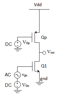
In our common-source amplifier, a primary goal of our active load is to provide a high small-signal impedance (translating to a high gain) while having only a modest large-signal voltage drop across it at the operating point (also called quiescent point in some texts).
In order to achieve this, we can use a MOSFET configured for nearly constant current, i.e. a MOSFET configured as the output side of a current mirror (or a constant Vgs in a simplified design/analysis).
The complication is that the MOSFET that we fabricate is a nearly symmetric device (and in some models such as the tsmc18 which I am familiar with, fully-symmetric); the source is always the side of the channel with lower voltage for NMOS, and higher voltage for a PMOS.
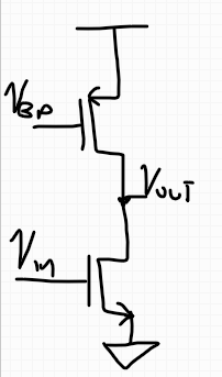
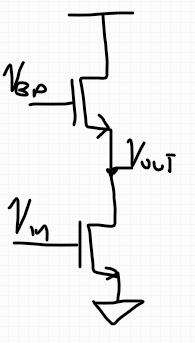
Compare these two topologies:


Notice which side ends up being the source (marked with the arrow). In the first topology (PMOS), the higher voltage is the source, and that's the rail. Perfect, because it means that our constant bias voltage \$V_{bp}\$ creates a nearly constant current through the drain, and the impedance seen looking into that drain is very high (it's the output impedance associated with channel-length modulation).
Now look at the second topology. The top FET is an nFET, meaning that its source is tied to the output. The impedance seen looking into the source is very low, because Vgs varies significantly as the amplifier's output voltage (i.e. the top FET's source voltage) varies. In fact, this active load is actively counterproductive -- it creates a feedback structure that tries to hold Vgs of the two FETs relatively similar to each other because they have the same current running through them. This makes it no longer amplify -- depending on the relative shape ratios of the top and bottom FETs it has a tiny bit of gain at best, or is a really bad buffer, or even attenuates.
Our active load doesn't meet our goals, and our amplifier also fails to meet its goals as a consequence.
