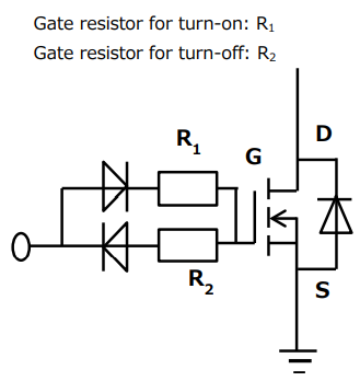
I am driving a STD3NK80Z-1 MOSFET at a rate of approximately 105kHz using the UCC28700 by TI, and I want to make sure my gate drive circuit is correct. I am going to use the schematic below as a starting point.
First, let's start off with an explanation of the schematic, so we can make sure my understanding is correct.
R1's job is to limit the in-rush current, and keep the drive pin from going over it's current source capacity. R2's job is to dampen the ringing observed when the gate signal goes from hi to low - basically just solving an RLC circuit.
In my case, the UCC28700 self-limits the source current of the DRV pin to 25mA, so I don't need to worry about placing a current-limiting resistor.
For R2, I found an equation in TI's "Fundamentals of MOSFET and IGBT Gate Driver Circuits"
Rgate,opt = 2*sqrt(Ls/Ciss) -(Rdrv + Rg,i)
I just plugged my numbers into that equation, and got a value of about 6.5 ohms.
At 14V (the drive pin's voltage), 6.5 ohms won't limit the current enough to reduce it below the self-limiting value, so I can just place it in series with the gate pin of the FET.
As a result, I will not need either of the diodes because current can flow through the resistor during the on phase and the off phase. This results in just a single resistor in series with the gate pin of the MOSFET.
My questions are:
- Is my understanding of the functionality of the two resistors correct?
- Is that a good value for R1?


R1is well chosen, if you can replace everything with only one resistor, other reason? \$\endgroup\$