1
\$\begingroup\$

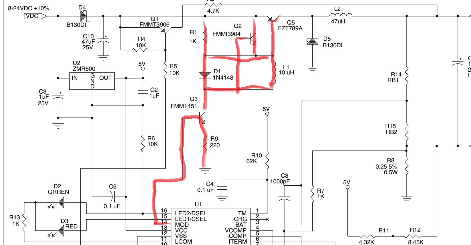
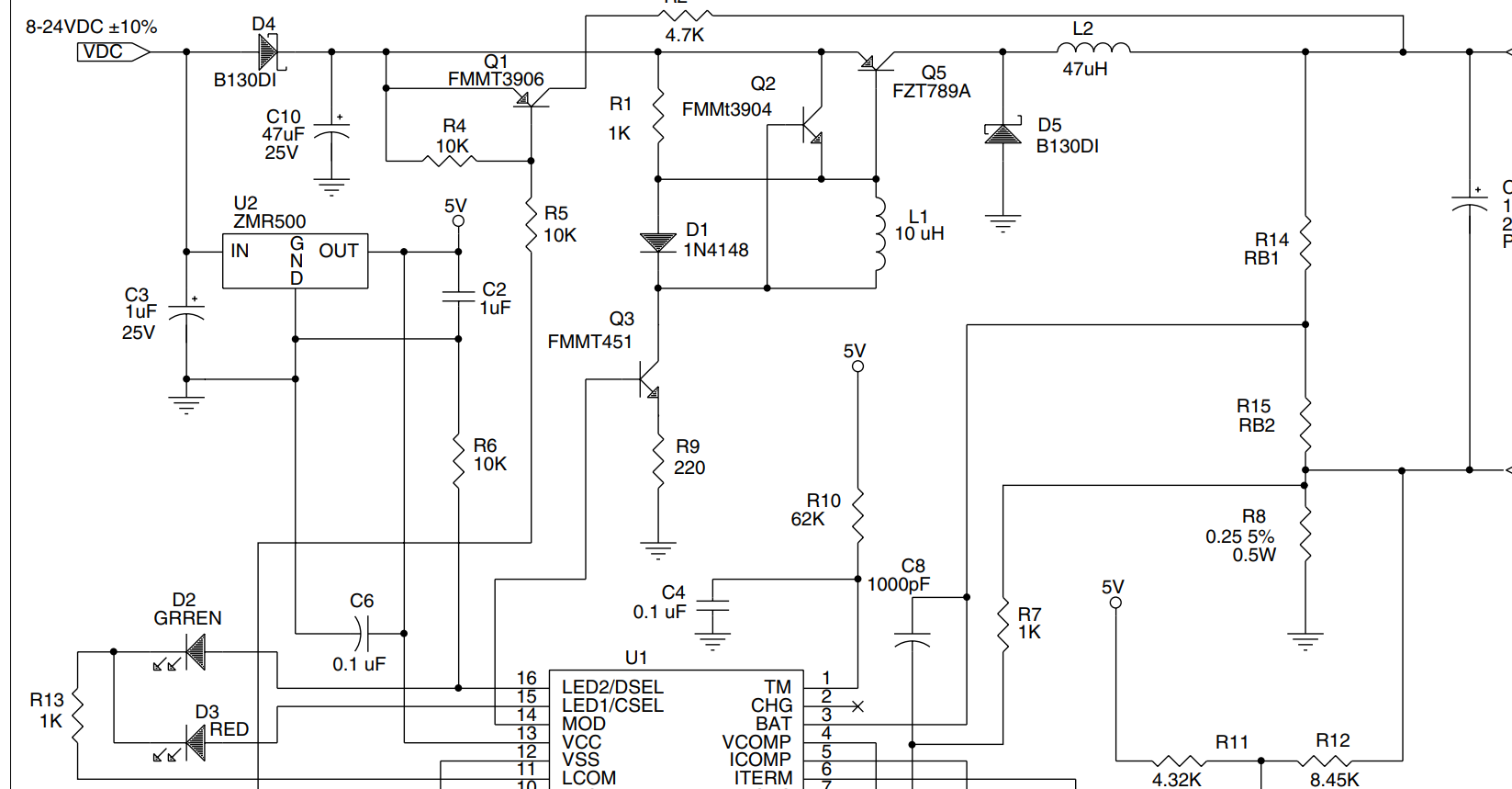
Can someone explain how this part of the circuit works? Why do they use PNP (Q5), NPN (Q2, Q3) transistors with inductor (L1) and diode (D1)? The Li-ion charger is a BQ2954.

The description for pin 14, MOD says:

Current-switching control output

Pulse-width modulated push/pull output used to control the charging current to the battery. MOD switches high to enable current flow and low to inhibit current flow. (The maximum duty cycle is 80%.)

Highlighted part

Original scheme

Thank you for help.

\$\endgroup\$
14
  • 1
    \$\begingroup\$ Looks like a power-shutoff to me. What is IC U1?? When Q3 is "on" (MOD is HIGH) then Q2 will be "off" and Q5 will be "on". This allows power to get to L2 and beyond. Send MOD low, Q3 will turn off, which in turn will turn Q5 off and cut the power. Not sure about Q2, looks like maybe it's purpose is to speed-up the turn-off time of Q5 by giving a path for it's internal capacitance to bleed off, but that's just an educated guess. The diode may serve to make sure Q2 is fully "off" (it will force Q2's base to be 0.7V below it's emitter) \$\endgroup\$
    – Kyle B
    Commented Jan 26, 2021 at 21:34
  • 1
    \$\begingroup\$ Ahh... I see the mention of which IC now ;) Sorry I missed that first! I didn't make it answer because somebody will undoubtably analyze this circuit (with numbers!!!) and I wasn't prepared to do that. I just wanted to give you a quick qualitative reply 'cuz I saw you just recently posted the question. (I know I'd be itching for an answer!) But stop back a few times, see what others say.... \$\endgroup\$
    – Kyle B
    Commented Jan 26, 2021 at 21:54
  • 1
    \$\begingroup\$ Looks like a buck converter to me. Q5,D5 and L2 form the buck converter. The rest is level translation and drive for Q5 \$\endgroup\$
    – Kartman
    Commented Jan 26, 2021 at 22:02
  • 1
    \$\begingroup\$ That's a very old charge controller from the days when power FETs were much more expensive than bipolars. I believe L1 pushes base current into Q2 on turn-off helping to speed up the turn-off of Q5. That whole arrangement would be better replaced with a power FET (and maybe some drive circuitry) these days. Or better yet a more modern controller. \$\endgroup\$
    – John D
    Commented Jan 26, 2021 at 22:14
  • 1
    \$\begingroup\$ My guess is to speed up the turn off of Q5. CV and CC are done by the microcontroller as part of the buck control loop. \$\endgroup\$
    – Kartman
    Commented Jan 26, 2021 at 22:15

1 Answer 1

1
\$\begingroup\$

Q5. D5, L2 form a basic buck converter circuit.

Q3 on turns Q5 on via L1.
Also "charging L1.
Also turning Q2 off.

Q3 off stops turning Q2 on clamps Q5 base to emitter and turns Q5 off.

Q3 off stops turning Q5 on BUT does not provide a fast hard turnoff signal for Q5.
BUT
Q3 off stops turning Q2 off and
L1 is now no longer "charged" by Q3 so
L1 bottom end rings positive driving Q2 off and hard clamping Q5 off.

Once Q5 is off and Q2 is no longer driven hard on by L1 ringing R1 holds Q5 off and
Q2 is held off by DC be short via L1.

As others have said - nowadays a MOSFET would usually be used at Q5.

\$\endgroup\$

Your Answer

By clicking “Post Your Answer”, you agree to our terms of service and acknowledge you have read our privacy policy.

Not the answer you're looking for? Browse other questions tagged or ask your own question.